New research enables high-speed customization of novel nanoparticles for drug delivery and other uses.
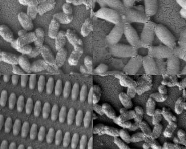
New research enables high-speed customization of novel nanoparticles for drug delivery and other uses.
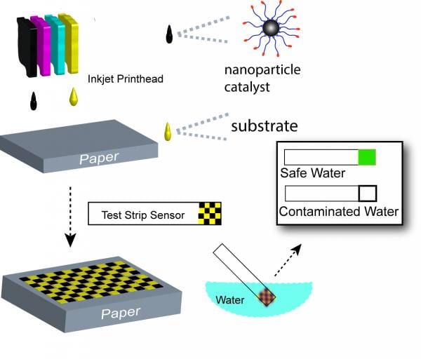
NAS announces grant to Vincent Rotelloto develop, test and deploy inkjet-printed, nanoparticle-based test strips for detecting bacteria in drinking water.
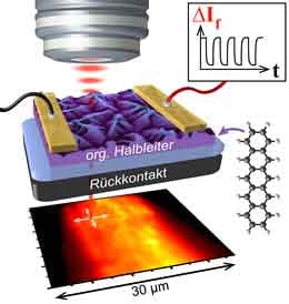
A team has, for the first time, succeeded in functionally characterizing the active layer in organic thin-film solar cells using laser light.
New hydrothermal atomic force microscope under development at Wright could hit 250 degrees.
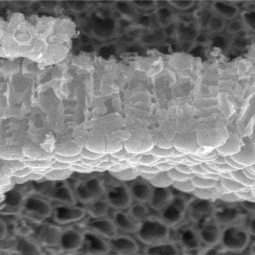
Scientists developed a convenient, anodization based method to produce a gradient TiO2 nanotube biomaterial.

Twelve partners from science, research, and industry joint together to develop kerosene from algae.
A colorimetric assay system based on urine and nanoparticles for mercury detection has been developed by researchers from Nanyang Technological University.
Organic semiconductor films are produced in regular arrays of inkjet-etched microwells, demonstrating potential for large-scale flexible electronics.
Research group from the Duke University develops a three-dimensionally woven fiber scaffold which mimics the properties of native cartilage.
Conference by IKV and ika on September 11 and 12, 2013 in Aachen.
 New theory suggests gravity is not a fundamental force
 Higgs boson may be driving the Universe’s expansion
 Water-powered gadgets may be on the horizon thanks to new evaporation-based energy device
 Scientists discover a new class of antibiotics
 Micron-sized hidden dimensions could solve two of physics’ deepest puzzles
 A new type of dark matter could explain mysterious radiation from the Milky Way’s core