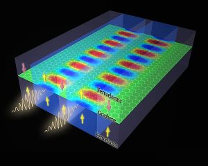
Schematics of a ferroelectric-graphene-ferroelectric nanostructure. Different domains of ferroelectrics can define densely packed waveguide patterns on graphene. Terahertz plasmons at ultrashort wavelength can flow on these waveguides. Image: Qing Hu.
Researchers at MIT have proposed a new system that combines ferroelectric materials — the kind often used for data storage — with graphene, a two-dimensional form of carbon known for its exceptional electronic and mechanical properties. The resulting hybrid technology could eventually lead to computer and data-storage chips that pack more components in a given area and are faster and less power-hungry.
The new system works by controlling waves called surface plasmons. These waves are oscillations of electrons confined at interfaces between materials; in the new system the waves operate at terahertz frequencies. Such frequencies lie between those of far-infrared light and microwave radio transmissions, and are considered ideal for next-generation computing devices.
The findings were reported by associate professor of mechanical engineering Nicholas Fang, postdoc Dafei Jin and three others.
The system would provide a new way to construct interconnected devices that use light waves, such as fiber-optic cables and photonic chips, with electronic wires and devices. Currently, such interconnection points often form a bottleneck that slows the transfer of data and adds to the number of components needed.
The team’s new system allows waves to be concentrated at much smaller length scales, which could lead to a tenfold gain in the density of components that could be placed in a given area of a chip, Fang says.
The team’s initial proof-of-concept device uses a small piece of graphene sandwiched between two layers of the ferroelectric material to make simple, switchable plasmonic waveguides. This work used lithium niobate, but many other such materials could be used, the researchers say.
Light can be confined in these waveguides down to one part in a few hundreds of the free-space wavelength, Jin says, which represents an order-of-magnitude improvement over any comparable waveguide system. “This opens up exciting areas for transmitting and processing optical signals,” he says.
Moreover, the work may provide a new way to read and write electronic data into ferroelectric memory devices at very high speed, the MIT researchers say.
Dimitri Basov, a professor of physics at the University of California at San Diego who was not connected with this research, says the MIT team “proposed a very interesting plasmonic structure, suitable for operation in the technologically significant [terahertz] range. … I am confident that many research groups will try to implement these devices.”
Basov cautions, however, “The key issue, as in all of plasmonics, is losses. Losses need to be thoroughly explored and understood.”
Source: MIT