28th International Colloquium Plastics Technology 2016: an international meeting place for the industry

28th International Colloquium Plastics Technology 2016: an international meeting place for the industry

Professor Ozin tackles one of the most popular metrics in modern science – the h-index.
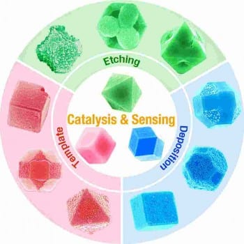
Facet-controlled synthesis strategies for Cu2O-based nanocrystals are reviewed and properties that make them suitable for numerous applications in sensing and catalysis are highlighted.

An international, interdisciplinary team is developing highly porous biomaterials for localised release of therapeutic ions and drugs
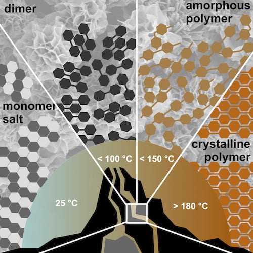
Miriam Unterlass investigates benign alternative polymerization process yielding polymers that are typically only conceivable under harsh conditions.

The accuracy of the Strain Energy Density averaged over a control volume approach when applied to high temperature fatigue data is investigated.
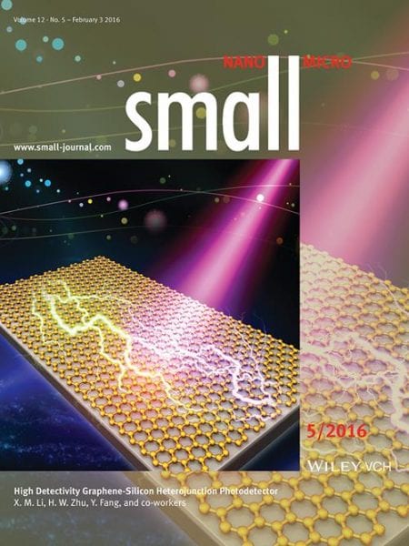
Researchers devise a highly detective photodetector based on graphene-silicon heterojunctions with interface improvement by introducing a thin interfacial oxide layer.
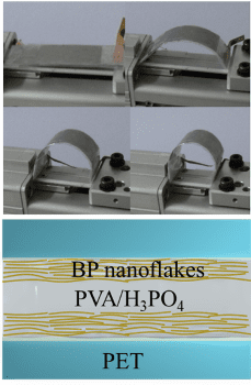
Researchers in China build powerful and durable all-solid-state supercapacitors using black phosphorus nanoflakes.
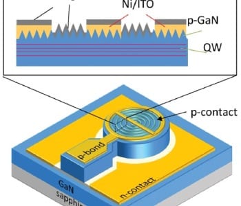
Enhanced recombination rate is achieved on a novel plasmonic platform that exploits the spontaneous formation of a V-pit-texture on the surface of a light-emitting diode.
Researchers at Sichuan University have created an alternative to conventional leather lubricants using synthetic copolymers.
 New theory suggests gravity is not a fundamental force
 Higgs boson may be driving the Universe’s expansion
 Water-powered gadgets may be on the horizon thanks to new evaporation-based energy device
 Scientists discover a new class of antibiotics
 Micron-sized hidden dimensions could solve two of physics’ deepest puzzles
 A new type of dark matter could explain mysterious radiation from the Milky Way’s core