Shu-Hong Yu and his team have developed a method to construct kinetically stable anode materials for high-energy applications.

Shu-Hong Yu and his team have developed a method to construct kinetically stable anode materials for high-energy applications.
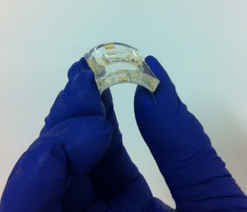
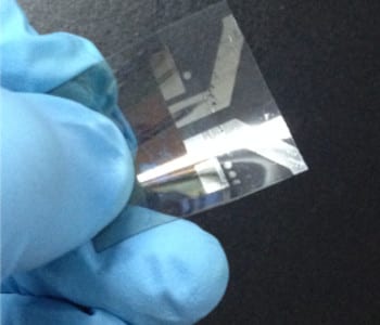
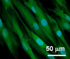
Researchers have created a low-cost, flexible bioelectronic device based on PEDOT:PSS, which they used for monitoring action potentials from cell tissues.
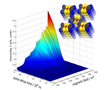
Joris van Slageren´s research group discovers molecular quantum bit with exceptionally long coherence time over an unusually wide temperature range.
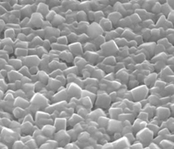
Researchers have formed perovskite films from a seed layer grown with atomic layer deposition, an standard technology for dielectric materials.
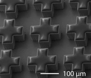
Cheng, et al. have created a broadband perfect absorber for terahertz waves by etching doped silicon to form micro-scale resonant cavities.
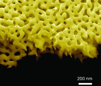
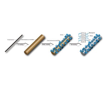
New research has found that “edge-free” monolayer MoS2 films supported by 3D nanoporous gold possess outstanding catalytic activity,
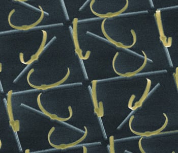
A collaborative team of researchers has reported pioneering work to create an isotropic infrared metamaterial consisting of 3D metallic nanostructures.
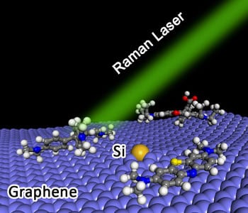
The Terrones group at The Pennsylvania State University in the US has reported a controlled technique able to dope graphene with silicon atoms.
Nanostructuring improves optical confinement and limited light out-coupling efficiency from by the mismatched refractive indices of media in devices.
Researchers have successfully fabricated titanium surfaces chemically functionalized with the flavonoids taxifolin and quercitrin.