 Perovskite thin films are an exciting class of semiconductor materials with great promise in third-generation solar harvesting technology, as well as in light-emission and detection. In contrast with most modern electronics, these semiconductor films can be deposited via inexpensive and facile methods at low temperature and pressure, enabling compatibility with flexible substrates.
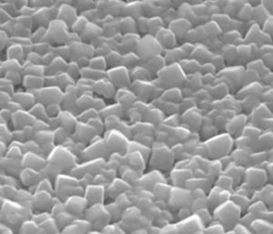
Researchers have now developed a method to form perovskite films from a seed layer grown with atomic layer deposition, an industry-standard technology for high performance dielectric materials. A chief benefit of atomic layer deposition is the capability to deposit thin-films onto highly structured substrates, with good adhesion and infiltration. The group demonstrated that perovskites grown in this way show great promise for optical amplification, with gain coefficients comparable to that of crystalline semiconductors and have exciting prospects for new optoelectronic devices leveraging the conformal capabilities of this technique.