Cheng, et al. have created a broadband perfect absorber for terahertz waves by etching doped silicon to form micro-scale resonant cavities. Instead of using metal-based resonances that have relatively low loss for terahertz waves, the structure relies on lossy plasmonic resonances for energy dissipation. In effect, the absorber exhibits an exceptionally high level of absorption.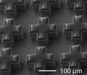
By combining two plasmonic resonances together, the absorber can achieve an absorption bandwidth up to 90%. Further, the employed single-layered structure is far superior to those broadband multilayered absorbers in terms of fabrication simplicity, and hence is appealing for a range of applications including terahertz communications and imaging.