Self-adaptive complementary-like architectures are adopted in graphene-based transistors as a means to create low power, high gain logic gates.
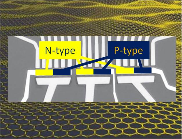
Self-adaptive complementary-like architectures are adopted in graphene-based transistors as a means to create low power, high gain logic gates.
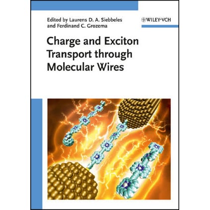
New publication brings together theory and experimental results in molecular electronics – can we go beyond Moore’s law? Emanuele Orgiu & Paolo Samorì of ISIS tell us more
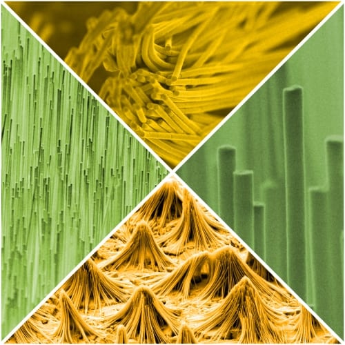
One-dimensional nanostructures like nanowires, nanobelts, and nanotubes attract considerable interest. However, common techniques to separate the nanostructures from the template can cause the structures to collapse.
Very small organic thin-film transistors with high operating frequencies have been produced by Japanese and German scientists.
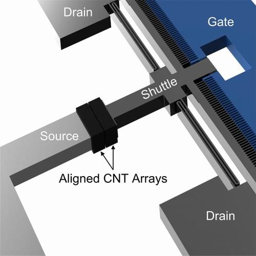
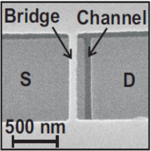
Korean researchers make a tiny switch from carbon nanotubes.
ZnSe is deposited in silica pores to produce the first compound semiconductor optical fiber waveguides.
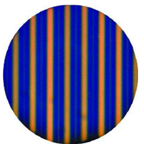
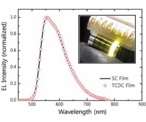
Two dyes give three colors on a hierarchically patterned surface, in work by German and Chinese scientists.
A novel polymer processing methodology to prepare thin films allows for increased crystallinity giving rise to improved properties.
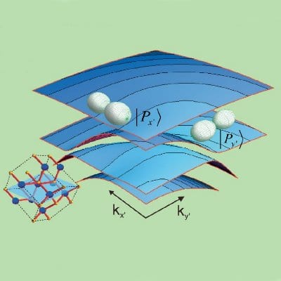
The research group “PolarCon” publishes a collection of papers describing the technological challenges of epitaxially grown non- or semipolar nitride structures.
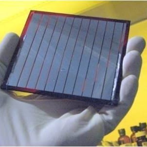
What is the ideal nano-morphology for organic and hybrid solar cells? A progress report from a German research group sheds light on recent developments.
 New theory suggests gravity is not a fundamental force
 Higgs boson may be driving the Universe’s expansion
 Water-powered gadgets may be on the horizon thanks to new evaporation-based energy device
 Scientists discover a new class of antibiotics
 Micron-sized hidden dimensions could solve two of physics’ deepest puzzles
 A new type of dark matter could explain mysterious radiation from the Milky Way’s core