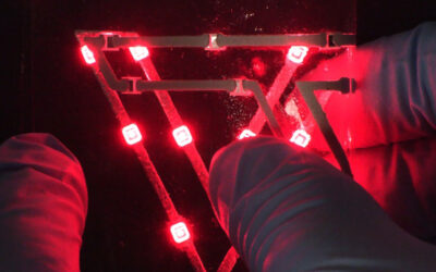
 Graphene, single atomic layers of graphite, opens up the manufacture of promising new materials and innovative electronics. Graphene transistors are predicted to be substantially faster than conventional silicon transistors and could lead to more efficient computers. Kostya Novoselov and Andre Geim from the University of Manchester (UK) first isolated graphene in 2004. For groundbreaking experiments regarding graphene, they were awarded the Nobel Prize in 2010.
To build up electronics from graphene, nanostructures can be carved out, which, most commonly, is done by electron beam lithography with subsequent etching in reactive ion plasmas. A promising alternative is given by atomic force microscopy (AFM)-based local anodic oxidation (LAO), also referred to as scanning probe lithography. In a special issue of physica status solidi (b), Novoselov and his colleagues outline the principles of this technique and demonstrate that it provides a resolution good enough for creating nanoelectronic device structures.
The special issue is based on contributions from the 24th International Winterschool on Electronic Properties of Novel Materials: “Molecular nanostructures”, which took place in March 2010. It was focused on topics such as carbon nanostructures, graphene, fullerenes, endohedrals, fullerides, graphite, non-carbonaceous nanostructures, nanotube optics, molecular electronics, quantum interactions, and nanotube devices.
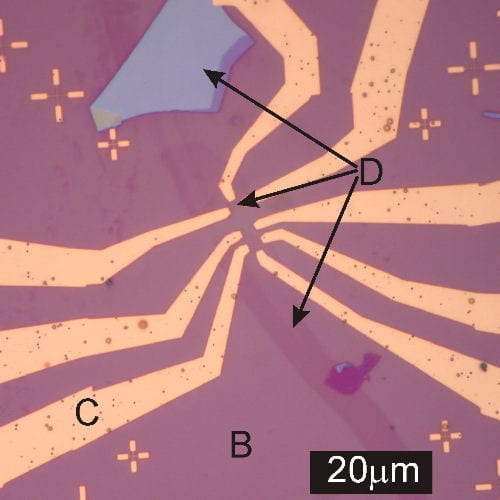
Novoselov, being a member of the Winterschool’s Program Committee, showed several examples of structures etched in graphene, including an example of a nanoelectronic device. He and his team were able to create lines as thin as 30 nm. Examining the lines, they found that the oxidized areas, when imaged in contact mode AFM, sometimes appeared as protrusions and sometimes as depressions, depending on the scan direction. This might be due to frictional forces on the contact AFM imaging process. To solve the question whether they created a stable graphitic oxide, or whether they etched away the graphene completely, they took tapping mode AFM images of the etched lines. The improved lateral resolution allowed distinguishing areas for some of the lines where graphene was etched away and where residual pieces of oxidized graphene remained. Obviously, prolonged exposure to the tip voltage leads to the eventual removal of graphene.
Having established the working parameters for AFM-based lithography of graphene, they focused on oxidizing nanometer-sized structures that could operate as nanoelectronic devices. As an example, they created a quantum point contact with adjacent sidegate oxidized in graphene. The quantum point contact was a region of intact graphene with a size of about 60 nm X 60 nm.
The team also presents data regarding the oxidation kinetics when performing scanning probe lithography on graphite (HOPG), finding a dual-reaction pathway kinetics resembling the one observed for LAO on silicon. This leads to the conclusion that a stable oxide is selectively created on HOPG. For LAO on graphene, the results obtained on HOPG indicate that the oxidized areas consist of a graphitic oxide. But since graphene has a thickness of only one atomic layer, the possibility of a complete etch cannot be ruled out strictly.

