Researchers describe the experimental realization of an optical switch controlled by a single photon, allowing light to govern the transmission of light.
Researchers describe the experimental realization of an optical switch controlled by a single photon, allowing light to govern the transmission of light.

What materials discoveries had an impact on business the past 10 years? How will we do materials science startups in the future? Jeff Carbeck explains.
Organic semiconductor films are produced in regular arrays of inkjet-etched microwells, demonstrating potential for large-scale flexible electronics.
The world’s most advanced extreme-ultraviolet microscope is about to go online at theDOE’s Lawrence Berkeley National Laboratory.
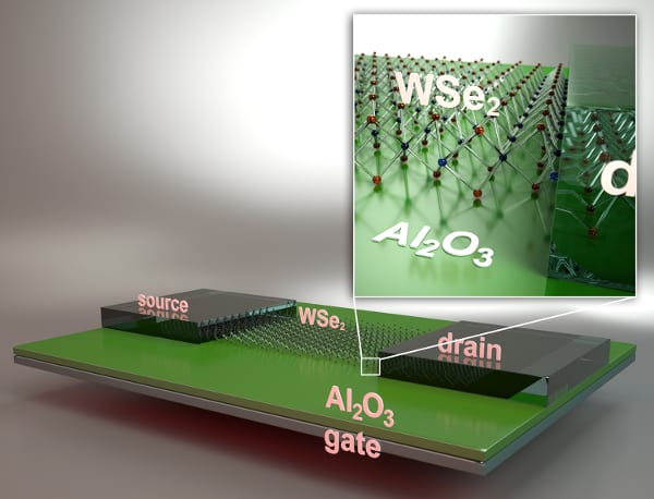
UC Santa Barbara researchers demonstrate first n-type field effect transistors on monolayer tungsten diselenide with record performance.
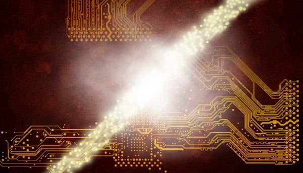
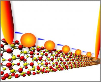
Scientists have discovered how optical signal transmission can be controlled, which could lead to integration of plasmonics with electronic circuits.
New electronics harness quantum tunnelling to create transistors without semiconductors.
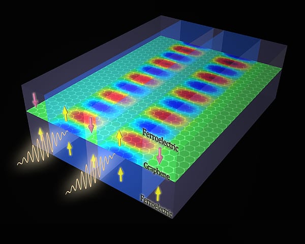
New system uses two-dimensional structures to guide plasmonic waves at ultrashort wavelength, offering a new platform for memory and computer chips.
Technique developed several years ago at NIST for improving optical microscopes could be applied to the next generation of computer chip circuit components.
Siemens scientists have developed new kinds of ceramics in which they can embed transformers.

 New theory suggests gravity is not a fundamental force
 Water-powered gadgets may be on the horizon thanks to new evaporation-based energy device
 Micron-sized hidden dimensions could solve two of physics’ deepest puzzles
 Turning Periods into Power: Menstrual Blood a Valuable Resource for Medical Diagnostics
 Organic materials bring probabilistic computing closer to reality
 Kirigami-inspired neural probes are a cut above