The world’s most advanced extreme-ultraviolet microscope is about to go online at the U.S. Department of Energy (DOE)’s Lawrence Berkeley National Laboratory (Berkeley Lab), and the queue of semiconductor companies waiting to use it already stretches out the door.

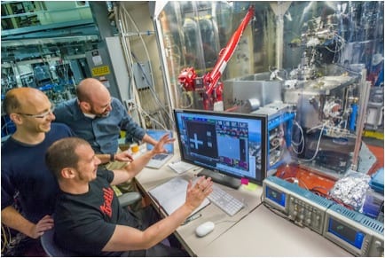
Goldberg, with team members Iacopo Mochi and Markus Benk, gather around the control center for the SHARP microscope, an extreme-ultraviolet-wavelength microscope dedicated to photomask imaging for the commercialization of EUV photolithography.
The much-anticipated SHARP microscope (SEMATECH High-NA Actinic Recticle review Project) was conceived and built by scientists at Berkeley Lab’s Center for X-ray Optics (CXRO) and will provide semiconductor companies with the means to push their chip-making technology to new levels of miniaturization and complexity. The instrument is housed at the Advanced Light Source (ALS) at Berkeley Lab, widely known as one of the world’s preeminent laboratories for extreme-ultraviolet (EUV) research.
SHARP replaces an older tool, also located at the ALS, and has been many years in the making. Kenneth Goldberg, a researcher in Berkeley Lab’s Materials Sciences Division, and deputy directory of CXRO, runs the project.
“With the old tool we suffered greatly just to squeeze good results from it,” says Goldberg. “We always talked about what we’d do if we had the chance to do it right.”
Goldberg and his colleagues got that chance thanks to a partnership with SEMATECH, a consortium of semiconductor companies and chip-makers who recognized in CXRO the ideal combination of resources and expertise. The collaboration is part of a long-standing partnership between CXRO and SEMATECH that serves as a model for how industry and National Labs can combine forces to address critical challenges for the semiconductor industry. SEMATECH’s constituent companies are interested in developing EUV fabrication techniques in order to shrink circuit elements in their computer chips down to a few nanometers in size – five to ten times smaller than they are today.
In semiconductor fabrication, circuits of silicon are made via photolithography.

Created by the Center for X-Ray Optics at Berkeley Lab, SHARP gives researchers from the world’s leading semiconductor companies a window into the future of computer-chip fabrication.
“Photolithography works like darkroom photography, where an image on film is enlarged and projected onto light-sensitive paper,” says Goldberg. “But in photolithography you flip the optics backwards and shrink an image of a circuit from a mask down onto a silicon wafer coated with light sensitive film. So you want to use all the physics you can to make those circuits as small as possible.”
Physics says that the smaller the wavelength of light you use, the smaller the pattern you can draw, which is why the chip industry has moved from using visible light to ultraviolet to deep-ultraviolet over the past four decades. Now by shifting to EUV light, with a wavelength 15-times smaller than current techniques, researchers hope to make circuit elements on the nanometer scale, but that also requires a new level of perfection in the photolithography masks.
The SHARP microscope was built to examine defects in photolithography masks 10-40 nanometers wide – tiny, but big enough to interfere with circuit elements of similar size. The usual inspection tools, such as electron and atomic microscopy, can’t predict the impact of such defects on EUV wavelengths, which is necessary to make successful repairs.
One of the great advances of SHARP, compared to its predecessor, is the flexibility to emulate all current and future EUV illumination setups.
“This tool will let companies look way into the future,” says Goldberg. “Whatever they can dream as a future set up, they can test with our tool.”
SHARP is also dramatically more powerful and accurate than its predecessor. Goldberg and his team improved the optical efficiency 150 times, and took great pains to insulate the tool from mechanical vibrations. Eventually, the whole setup will go into a thermo-acoustic shell for further shielding.
Technological feats aside, the project has also brought a huge sense of accomplishment to the CXRO team.
“It has been so fun to be a part of this project,” says Goldberg. “It’s been one of the most creative periods in my life, and I’m so proud of what our team has accomplished. I have a huge sense of pride now to watch the tool produce great results.”
Recently the team hit a big milestone, when they ran SHARP through a series of “acceptance” tests prior to taking it online for users.
“It got all As and a couple Bs,” said Goldberg, “but we can improve it based on those tests. We’ll learn and get better over time. That’s how we work.”
Source: Berkeley Lab

