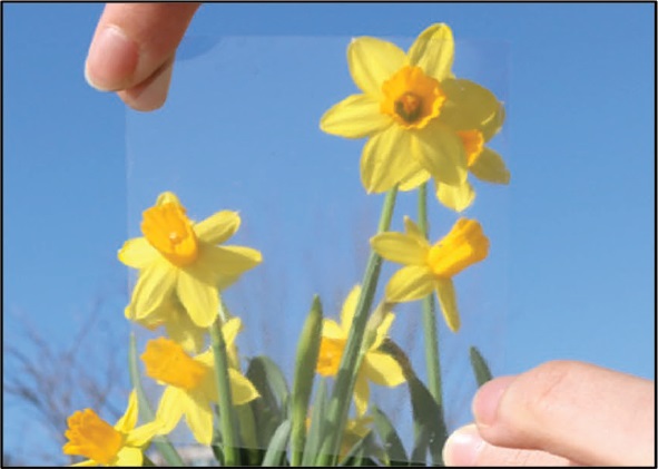
The device created with silica nanoparticles and projector slide film was up to 97% transparent.
Capacitive pressure sensors – the technology behind touchscreen functions in mobile electronics and other touch-sensitive devices – are becoming increasingly sophisticated.
A capacitor is traditionally formed from a dielectric layer sandwiched between two conducting electrode plates. The plates accumulate and store electric charge; the dielectric is an insulating layer. As the capacitance of a device is inversely proportional to the distance between the two conducting plates, applying pressure to one of the plates (thereby decreasing that distance) can generate a measurable change in capacitance. This is the basis for a pressure-sensing device.
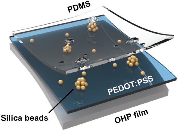
Device architecture for the new capactive pressure sensor.
The desire to extend the application of touch-sensitive devices by also making them flexible and transparent – such as for the recent, very popular electronic skins – has forced the investigation of new materials and increasingly creative device structures. With that in mind, researchers from Yonsei University and Korea University have developed a pressure sensor with up to 97% transparency by dispersing nanoparticles (as the conducting elements) throughout a polymer composite dielectric matrix.
To create their device, they started with 500 nm silica spheres dispersed throughout a PDMS layer as a mixture of individual particles and larger aggregates. This layer was sandwiched between two PEDOT:PSS layers and a transparent and flexible film, originally produced as a commercial overhead projector slide, was used as a substrate.
Different sizes of particles were tested, with larger particles expected to produce better results due to the generation of an air gap at the interface. This gap produces a surface roughness that increases the compressibility and therefore the capacitive sensitivity of the device (as defined in their Communication, published in Small). Surprisingly, then, the 500 nm particles produced a significant increase in sensitivity as compared to their microscale counterparts, achieving 1.0 kPa-1 versus 0.44 kPa-1 for the most sensitive microparticle-based devices.
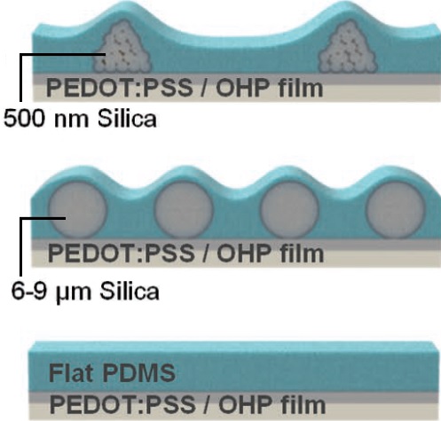
Particle size affects the surface roughness of the PDMS layer, which changes the sensitivity of the device.
This result was attributed to the aggregation of particles, creating larger ‘bumps’ in the PDMS layer, and therefore a rougher interface.
The researchers suggest that their approach experimentally verifies that such processing techniques are “effective on the nanoscale, yet applicable to macroscopic processing”, which is important for the industrial uptake of this technology. They demonstrate a range of applications, including attaching a modified version of their device (with a plastic wrap substrate, for even greater flexibility) to a blood vessel for real-time monitoring, and the creation of a fully functional transparent, flexible keyboard.
Such increased transparency and flexibility can remove the boundaries between people and technology, and facilitates the integration of this new device for a wide range of applications.
Interested in the latest news on flexible electronics? Why not check out this recent research: