What does cooking in your kitchen have in common with printed electronics? More than one would think!
Sintering is a widely used technique for bonding particles into coherent structures, imparting increased strength and integrity. Due to its low cost, and reliability, thermal sintering is broadly used to create metallic nanoparticle inks, which are used extensively in the printing of electronic devices, sensors, and light emitting diodes.
Though extensively used, thermal sintering is time-consuming and requires temperatures between 100 °C and 300 °C to render the metallic nanoparticles conductive. As a result, fabrication time is significantly increased in the additive manufacturing of electronics and the number of usable substrates is very limited.
Researchers have found various ways of selectively sintering for printed structures, i.e., only the nanoparticles are heated and not the underlying, perhaps temperature sensitive, substrate. For example, by chemical treatment, exposure to a laser beam, intense pulse light, microwave radiation — yes, that is a common kitchen microwave! — or the combination of two sequential sintering techniques.
While many do solve the time and temperature issues in thermal sintering of metallic nanoparticle inks, they are technically complicated and expensive. In addition, current sintering techniques are unable to satisfy all four main criteria for efficient protocols: short sintering time, selective sintering, excellent electrical conductivity of the sintered patterns, and not damaging to both substrates and printed patterns.
For instance, the intense pulse light sintering technique may cause undesirable defects in the sintered patterns, deteriorates the materials’ properties, which requires much post-printing optimization. The laser sintering process is also not ideal for sintering large areas with low writing speed, and the laser beam is only able to induce its energy onto the materials with limited penetration depth. Although the microwave sintering technique can sinter metallic particles in a relatively short time, the microwave energy only also has a limited penetration depth of a few microns on the printed patterns and may not be ideal for sintering thick printed patterns.
To overcome these challenges, a research team led by Professor Chua Chee Kai from the Singapore University of Technology and Design has developed a novel and robust induction sintering technique that solves the major challenges faced by the current techniques in sintering metallic nanoparticle inks. Their study was recently published in Advanced Materials Technology.
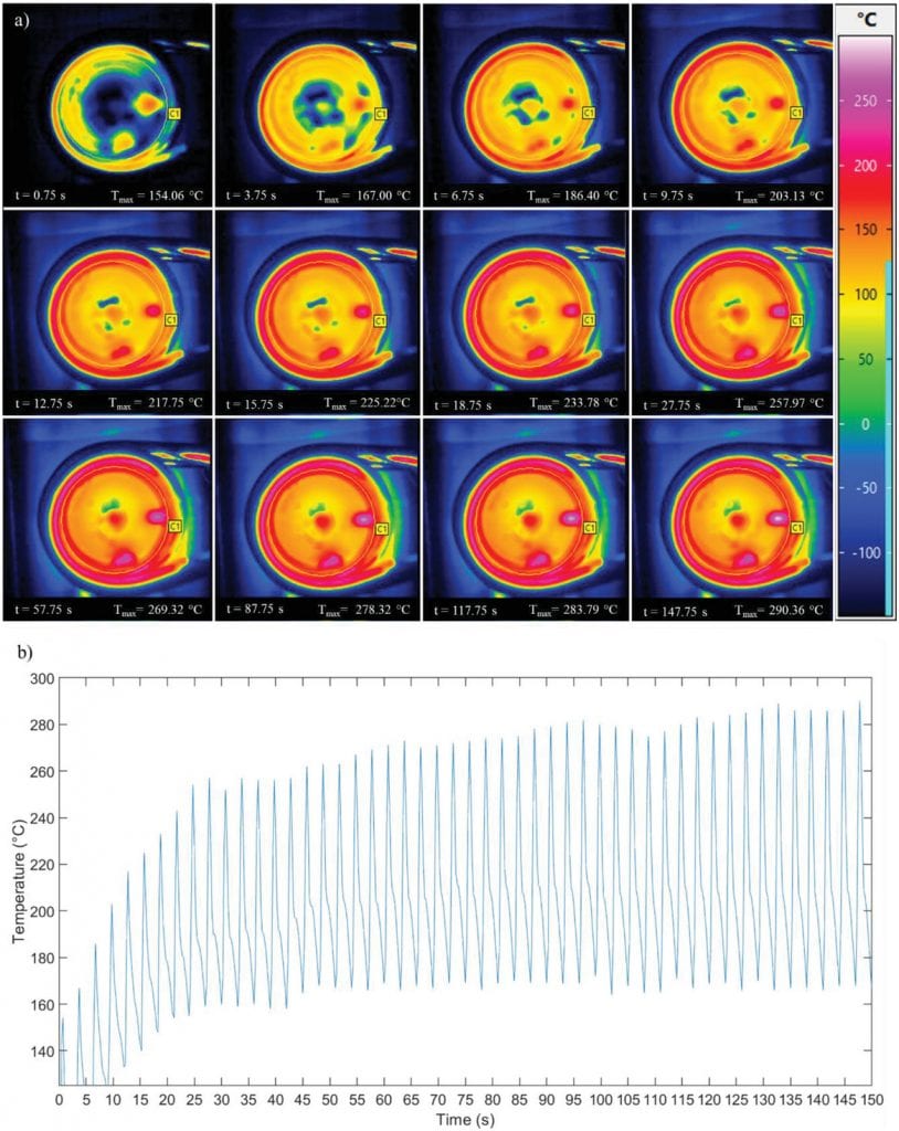
The induction sintering process used here is the same as induction-based stovetops found in modern kitchens; it is a non-contact, selective sintering process in which only electrically conductive pre-sintered, printed patterns are heated by alternating electromagnetic field through eddy current losses. It is also more energy-efficient and effective as compared to thermal sintering since it only heats only the electrically conductive printed patterns rather than the entire substrate. After sintering, the electrical resistivity of the induction sintered printed patterns was measured to be approximately 81% bulk conductivity of silver. This is the highest demonstrated bulk conductivity compared to other sintering processes.
“Our breakthrough research in pioneering the use of induction heating for sintering metallic nanoparticles while achieving the highest bulk conductivity compared to current conventional sintering methods, will pave the way for experts from academia and the industry to fabricate more reliable and consistent electronic devices,” adds Kai.
It’s quite interesting that the induction technique used widely in our kitchens is now being used as an advanced sintering technique. Due to its simplicity, it will likely have a major impact in printed electronics where conductive connections are essential.