 Photonic crystals (PCs) are materials that can be used to manipulate the propagation of light. Three-dimensional PCs produced by existing fabrication methods are of a passive nature with fixed optical properties, which means that any requirement of a slight optical change, such as in solar cell, light emitting diode or lasing applications, will generally need the fabrication of a new photonic crystal.
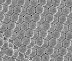
Now a group has reported a new approach which enables precision-tuning of the optical properties of PCs on the nanometer scale. As PCs are porous structures which contain an extensive network of inter-connected air voids, very thin layers of polymeric materials have been deposited on the surface of the pores in a layer-by-layer fashion, leading to nanometer-tuning of the PC optical properties. The approach is facile and reproducible, and key to it is the use of polyelectrolytes which possess controlled short chain lengths with narrow polydispersity. This ensures that the polyelectrolytes are small enough in size that they do not block the air voids during the early stages of the deposition, thereby maintaining uniform coating throughout the entire PC structure. The precise and reproducible optical-tuning thus achieved is expected to be applicable to both ordered arrays as well as amorphous photonic media.