Micro- and nanoscale structures are essential in electronic devices and circuitry. The most commonly used technique to create such structures is by using photolithography, which has enabled the creation and mass-production of structures on the nanometer scale. With this technique, the semiconductor industry can produce wafers with hundreds of integrated circuits on a single wafer with a resolution of <10 nm, all within minutes.
While it has many advantages, one of the main limitations of standard photolithography is that all features are defined in one focal plane, meaning that patterning works only on flat surfaces. So, what if the surface is curved?
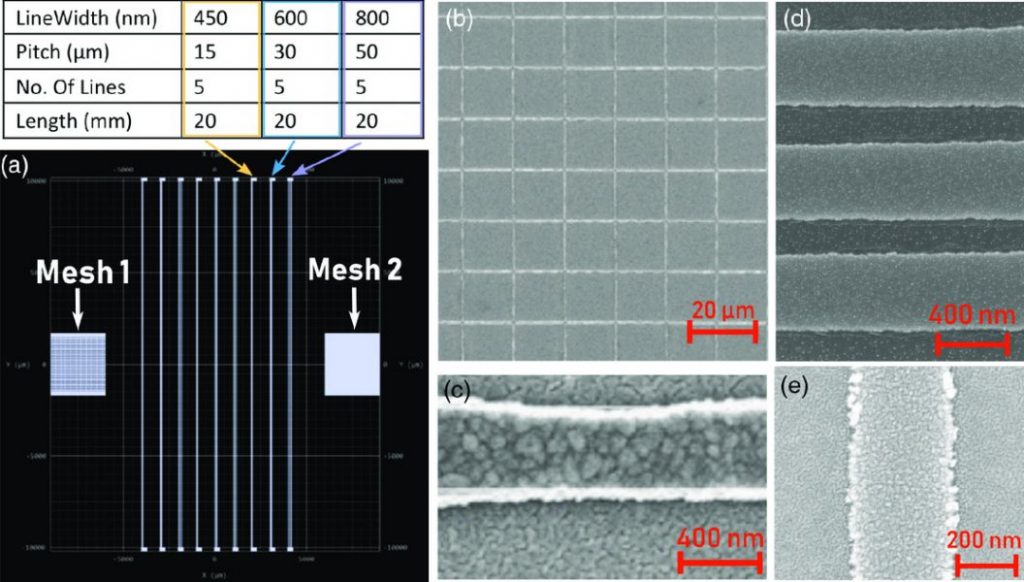
A possible solution to this was recently presented by Professor Ilari Maasilta from the Jyväskyla University in Finland. Maasilta and his research team show that one can still do photolithography in a special way, using a laser that has been focused into a small 3D spot that is controlled in the 3D space following elevation changes as high as 20 micrometers. This direct laser writing (DLW) technique enables the fabrication of sub-micron metallic wiring both up and down (see Figure 1).
Another method to produce metallic structures in the micrometer range is called additive manufacturing. The main driving forces behind this technique are the freedom of object size and design. However, the resolution of the design cannot be altered as the voxel diameter (voxel is the 3D version of a pixel) is usually fixed.
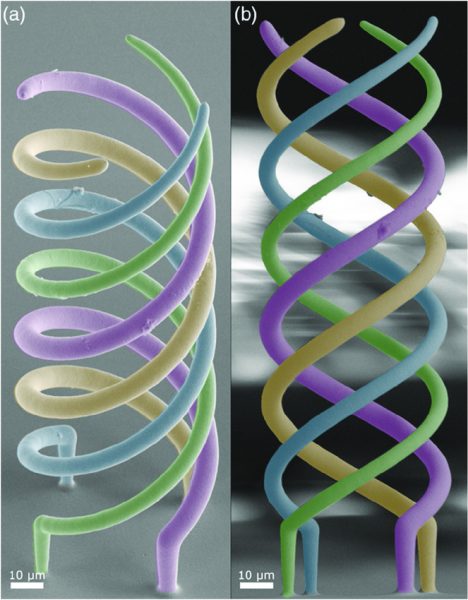
Adjusting the print volume on the fly, i.e., during the printing process, is what has been studied by Dr. Giorgio Ercolano, Professor Tomaso Zambelli and their colleagues at ETH Zürich, Switzerland. By adjusting the pressure which pushes the required liquid during the printing process out of the print nozzle, it is possible to increase or decrease the amount of liquid expelled onto the surface. As a result, an accurate control of the voxel area over two orders of magnitude is achieved.
The image to the right shows the structure containing four helical wires that was manufactured by changing the pressure on a voxel‐by‐voxel basis so that the four wires resulted each with a different diameter, but each homogeneous along the entire length.
These results show that additive micro-manufacturing of objects are now possible in object sizes starting below one micrometer, up to hundreds of micrometers in size. Additive micro-manufactured objects can support many research fields, from semiconductor to high frequency technology, or indeed any other fields where micro metal parts are required. The flexibility of the printable objects in shape and design provides a great opportunity for research facilities to manufacture objects on demand and in sizes not possible with any other technology. The next challenge is to combine various manufacturing technologies and to build fully functional parts with the new possibilities.
Research articles found at: S. Heiskanen, et al. Advanced Engineering Materials, 2020, doi.org/10.1002/adem.201901290; G. Ercolano, et al. Advanced Engineering Materials, 2020, doi.org/10.1002/adem.201900961