Modern day displays incorporated in smartphones and televisions increasingly include pixel technology based on organic light-emitting diodes (OLEDs), which turn electrical current into visible light. In an OLED, the organic semiconductor layers are sandwiched between two electrodes, of which at least one must be transparent to allow the light generated inside the device to escape. Most transparent conductive electrodes are based on indium tin oxide (ITO); however, its suitability for applications on non-rigid substrates is limited due to its brittle nature.
One suitable method of replacing ITO is through printed conductive structures deposited from a cost-effective metal nanoparticle ink such as copper (Cu), using a grid-like architecture to provide the necessary combination of conductivity and transparency. In order to merge the single nanoparticles into an interconnected conductive matrix, the deposited ink must undergo a curing treatment known as sintering. During this process, the oxidation of Cu must be avoided, as it strongly affects the conductivity. Many of the usual methods such as flash lamp and laser sintering require substrates with an appropriate thermal conductivity to avoid overheating, but these limit the substrates available for novel technologies.
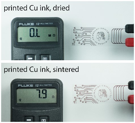
Dried printed Cu structures (top) showing no conductivity, while after low temperature sintering (bottom) the features are conductive.
The group of Prof. Emil List-Kratochvil from the Humboldt University in Berlin, Germany, have found a simple process using formic acid to create a reductive atmosphere, thereby preventing oxidation. “This reductive approach is widely used in the printed circuit board industry,” Dr. Felix Hermerschmidt explains, “and we have applied it for the first time using low sintering temperatures of 130 °C for solution-processed Cu-based structures, thereby also accessing flexible substrate types with low thermal stability, such as PET.”
The conductivity values reported are the highest in the literature for Cu structures at these low temperatures, and both the fabrication and sintering methods are suitable for large-area and high-throughput processing on flexible substrates.
As Prof. Emil List-Kratochvil points out, “through upscaling, these types of conductive structures can be produced at low cost and implemented in a wide range of applications, such as printed sensors and antennas, or as electrodes within more complex devices such as flexible OLEDs in wearables or packaging.”