 In dense metal nanostructure arrays with small interparticle distance, efficient focusing of light on the nanoscale can be achieved. It results in high local electric fields that can enhance optical processes at the metal surface. In principle, electron beam lithography can be used to fabricate regular nanostructured arrays, but the minimum achievable distance between particles is typically limited by electron backscattering.
Previous attempts to overcome this limitation require specialized fabrication approaches or particular structure designs. Now, in new research, a simple and general method has been developed to reduce interparticle distance in dense lithographically patterned arrays.
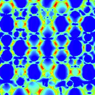
The approach involves repeated deposition and subsequent annealing of ultrathin gold films on top of pre-patterned gold nanoparticles. Surface diffusion of gold results in ripening of the initially patterned particles, thus reducing interparticle distance. The process can be tuned to realize a distinctly bimodal particle size distribution that is beyond the capabilities of any current lithographic method. Such a structure is suitable for focusing incoming radiation to a high density of nanoscale spots, with local field intensity enhancements up to three orders of magnitude compared to the incoming radiation, as confirmed by surface enhanced Raman scattering experiments and finite-difference time-domain calculations.


