Precise control over spatial composition during the fabrication of 1D materials is a challenge worth tackling, given the breadth of their potential applications. The ability to select an exact part of a 1D object and adjust its chemical, electrical, or magnetic properties would open up access to a new range of bespoke materials on this smallest possible scale.
Standard techniques, such as template-directed lithography, are potentially scalable at a low cost, but have been limited thus far by the homogeneity of the product: they’re only able to produce large batches of a single, unchanging type of material.
Researchers from Korea have now adapted the templated lithography technique to enable quite straightforward control over the morphological and chemical composition of 1D objects. Combining block copolymer lithography with an ion exchange process, they show how it is possible to reversibly alter the composition of arrays of metal nanowires at specific locations.
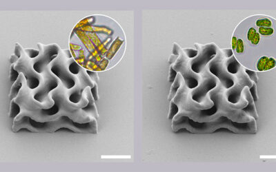
By sequentially loading desired metal ions into block-copolymer thin films and employing masks, metal ions can be replaced along selected segments of the formed nanowires. The researchers demonstrate their technique by fabricating platinum nanowires, and then selectively replacing the platinum with gold ions to form various patterns, and therefore regions, with different chemical properties. The image shows how, by rotating the masks, very different patterns can be created across large areas.
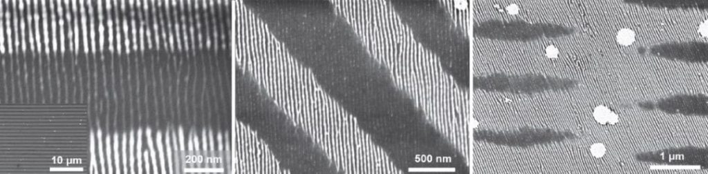
Scanning electron microscope images showing nanowires containing platinum (dark) and gold (bright) segments.
“Nanopatterned metal fabrication based on block copolymer self-assembly has been one of our principal research interests,” says Sang Ouk Kim, an author of the study. Nanopatterned metals display exploitable properties such as surface plasmon resonance as well as a certain tolerance for defect formation. “This quite contrasts from semiconductor nanolithography, which requires stringent control over minimal defect formation.”
The researchers envisage their technique being applied to create 1D materials of far greater morphological and chemical complexity than has previously been possible, without compromising any of the advantages lithography currently offers. “The possibility to fabricate metallic heterojunctions greatly broadens the potential of bottom-up nanoscale patterning,” confirms Sang Ouk Kim.
Could their method benefit your work? See the details of their photopatterning process now in Small.