The fundamental element of modern-day electronics is the field-effect transistor (FET), which relies on well-defined dielectric thin films on semiconductor substrates. Historically, sufficiently high-quality dielectrics for FETs have required vacuum deposition techniques, which are challenging to integrate with emerging roll-to-roll, solution-based manufacturing methods.
A research team at Northwestern University lead by professor Mark Hersam now has used 2D nanosheets of montmorillonite, which is a common earth-abundant layered silicate mineral, as the dielectric material. They could simply assemble these nanosheets from solution in a layer-by-layer approach to yield spatially uniform films of less than 10 nanometer thickness. Indeed, such dielectrics are efficient and possess high areal capacitances and low leakage currents.
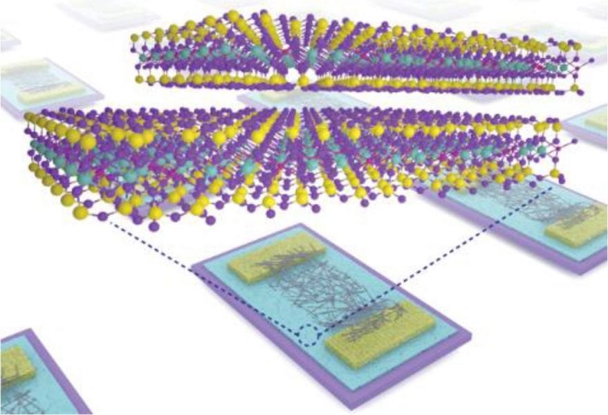
Scheme of the solution-processed field-effect transistors created from the dielectric thin nanosheet films.
Moreover, the scientists could employ the high-performance nanosheet films in solution-processed semiconductor field-effect transistors, based on carbon nanotubes or indium gallium zinc oxide, which both could be operated at low voltage. The promising results are likely to impact ongoing efforts to realize large-area flexible and wearable electronics through scalable additive manufacturing.
Full results and additional information are presented in the authors’ publication in Advanced Materials.