A new design approach and specialized organic material helps improve the efficiency of lateral solar cells, turning energy generation on its side.

A new design approach and specialized organic material helps improve the efficiency of lateral solar cells, turning energy generation on its side.
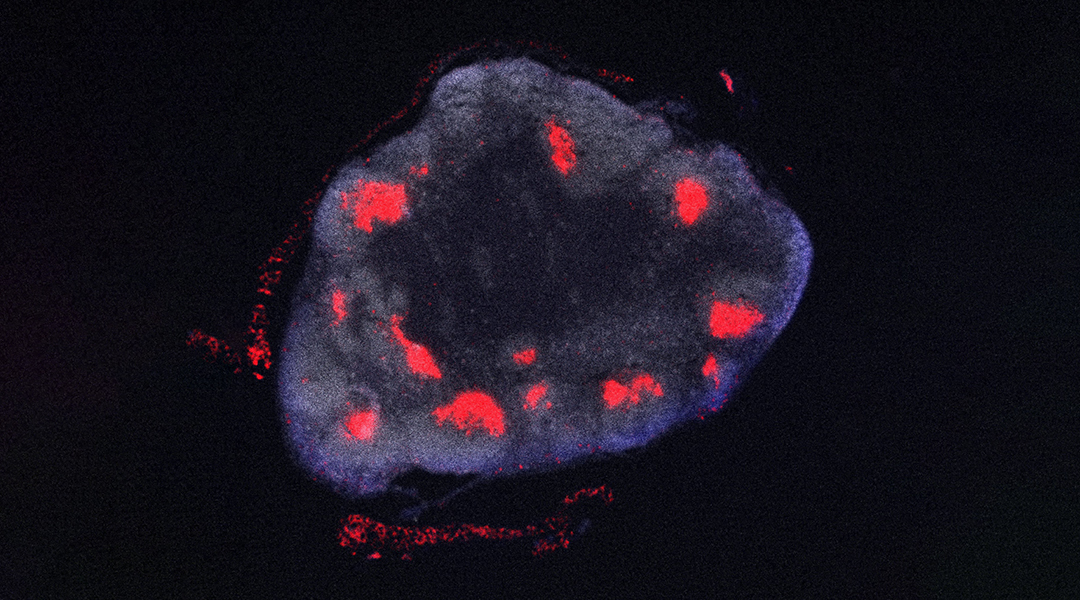
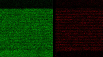
From boosterless vaccine platforms to goopy 2D inks and color-changing crystals, here are some of the most striking images collected from our journals.

Researchers use the ancient art of Kirigami folding to create flexible electronic devices from paper and diversify the applications of next-generation sensors, robots, and diagnostic devices.
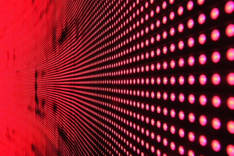
A new silicon-based light-emitting diode (LED) is developed, and provides a solution in the manufacturing of better LEDs.
New nitride semiconductors to expand the material toolset for infrared sensing devices.
The fabrication of indium-based microcolumns and nanowires with controlled phase and morphology.
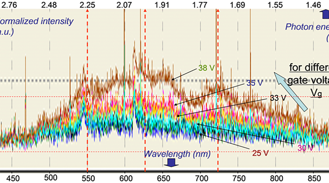
Harnessing light for practical applications requires small, versatile, and efficient optoelectronic devices.

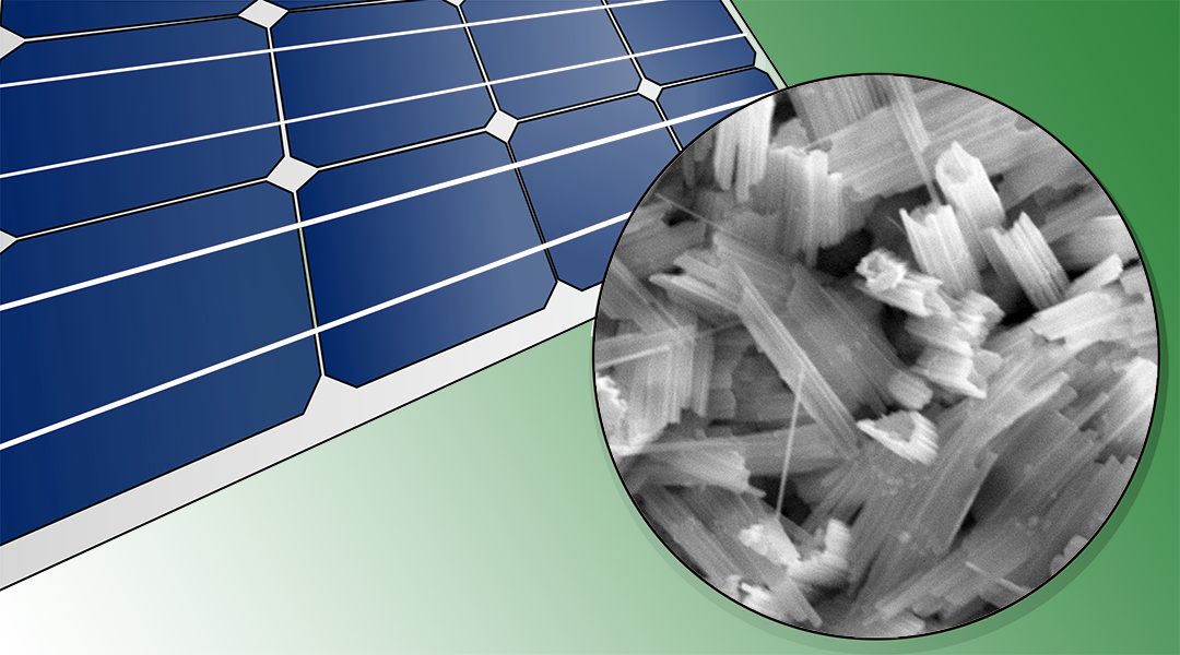
A new technique renders the low-cost process of sputtering a highly competitive fabrication method for photovoltaics.

Researchers have studied low-dimensional nanoscale ZnO building blocks, such as 1D nanorods, 1D nanowires and 2D nanosheets. Recently it was found that mixing these materials with 3D hierarchical ZnO microstructures revealed special optical, electrical and catalytic properties.
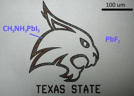
High-resolution photolithographic patterning of organohalide lead perovskites is made possible using hydrofluoroethers.

 Micron-sized hidden dimensions could solve two of physics’ deepest puzzles
 Turning Periods into Power: Menstrual Blood a Valuable Resource for Medical Diagnostics
 Surfactants Steer Supraparticle Structure
 Bone loss in obesity traced to gut microbiota
 Edible electronics realize safe, complex monitoring devices
 Fermilab Confirms Muon g-2 Measurements