Harnessing light for practical applications requires small, versatile, and efficient optoelectronic devices. The light-emitting diode (LED) revolutionized our world by enabling applications as dissimilar as LED light bulbs and fiber-optic telecommunications. Light beyond the visible range, in particular infrared light, holds the key to augmenting our senses. Infrared light is emitted by all objects at room temperature but, for this reason, it has been harder to control.
Oana Malis and team at Purdue University are designing, synthesizing, and studying new nitride semiconductors to expand the material toolset for infrared sensing devices.
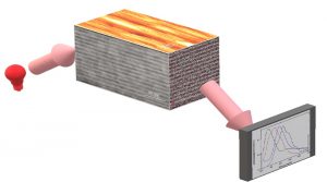 The nitride materials exploit the unique properties predicted by quantum mechanics at the nanoscale to interact with infrared light. AlGaN/GaN multilayers were grown by molecular-beam epitaxy (MBE) on two different GaN crystallographic axes (c-plane and m-plane) to examine the differences induced by crystalline orientation on structure and optical properties. MBE allows growth of hundreds of nanometer-thick layers with atomic precision under conditions far from equilibrium.
However, these materials test the limits of our fundamental knowledge about how they assemble and how electrons behave under the constraints of the atomic lattice. Infrared spectroscopy, and structural characterization with x-ray diffraction, atomic force microscopy and transmission electron microscopy, were used to correlate the optical and structural properties of the materials. The experimental results were also compared with numerical calculations.
Oana Malis and co-workers found that under identical conditions, the structures grown simultaneous on c- and m-plane surfaces are dramatically different. After reviewing the literature in the field, the authors concluded that future progress towards infrared light sources and detectors based on these materials depends on the ability to further optimize growth to alleviate current material issues related to homogeneity, and charge activation.
This article is part of a Topical Section on “Group III-Nitrides: fundamental research, optoelectronic devices and sensors” published in physica status solid (a).
Kindly contributed by the Authors, and modified by Marc Zastrow.