 Typical methods of direct patterning of ZnO films require long processing time, and expensive, multistep procedures. Researchers in Troyes, France have developed a cheap and efficient method of direct patterning ZnO films, using laser interferential lithography to selectively remove ZnO in well-controlled patterns, without the use of a photoresist. When immersed in a salt solution, ZnO is found to dissolve under UV light. This patterning method is therefore highly cost effective, as salt solution is a cheap raw material.
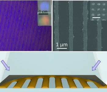
To demonstrate the technique, thin ZnO films were prepared on glass and silicon substrates, and immersed in a 0.1 m NaCl solution. The films were then exposed to UV light in a fringe pattern generated by laser interference. ZnO at the bright fringes was selectively dissolved, resulting in a structure of parallel lines being patterned into the film. The periodicity of the structure can be controlled by controlling the angle of interference of the laser beams. Additionally, more complex patterns, including dots, squares, and hexagons, can be obtained by rotation the film and further exposure steps. Longer exposure times lead to smaller structures, while no dissolution occues in the dark fringes. Direct patterning is achieved over large areas, limited only by the spot size of the laser beam.
The rate of dissolution of the ZnO film was found to be 0.7 nm min–1. The patterning process can be sped up by applying a bias voltage across the sample and the solution. The rate of the dissolution reaction can be spectacularly increased by up to 20 times, through application of a 0.6 V bias voltage. This faster dissolution was shown to yield patterned structures with reduced surface roughness.
Application of the bias voltage increases the separation of electron and hole charge carriers within the conduction and valence bands of the ZnO surface, where the reaction takes place. Electron–hole pairs are generated within the ZnO when irradiated by UV light of a higher energy than the bandgap. The hole carriers react with the ZnO to form Zn2+ ions, which combine with chlorine ions in solution to form ZnCl2.
The patterned ZnO film was then used to selectively grow ZnO nanowires, via chemical bath decomposition in an aqueous solution of zinc acetate dihydrate and ammonia. The nanowires grew only on the areas of remaining ZnO, at a uniform direction normal to the surface of the film. This demonstrates that this direct patterning method can be used as a full controlled chemical process for selective growth of ZnO nanostructures.
ZnO is a multifunctional material, with piezoelectric properties, a wide bandgap, large exiton binding energy, and high optical gain, as well as transparency in the visible region. Patterning of ZnO opens up further potential in these areas through the creation of periodic nanostructures, allowing use in photovoltaics, thermoelectrics, piezoelectrics and nanogenerators. The long processing times, laborious multi-step procedures of typical ZnO patterning techniques result in high costs, and cannot be scaled for large areas. This new, direct patterning method allows for fully controlled, large scale patterning at very low cost. The laser patterning method is also highly flexible, with a wide range of patterns that can be generated by laser interference.