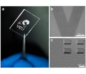
A wide range of patterns and features can be formed from silk proteins at small length scales. For example, microscale dots can be printed on glass to form a silk hologram. Image: Vamsi Yadavalli, Ph.D./VCU.
When most people think of silk, the idea of a shimmering, silk scarf, or luxurious gown comes to mind.
But few realize, in its raw form, this seemingly delicate fiber is actually one of the strongest natural materials around – often compared to steel.
Silk, made up of the proteins fibroin and sericin, comes from the silkworm, and has been used in textiles and medical applications for thousands of years. The Food and Drug Administration has classified silk as an approved biomaterial because it is nontoxic, biodegradable and biocompatible.
Those very properties make it an attractive candidate for use in widespread applications in tissue engineering. One day, silk could be an exciting route to create environmentally sound devices called “green devices,” instead of using plastics. However, forming complex architectures at the microscale or smaller, using silk proteins and other biomaterials has been a challenge for materials experts.
Now, a team of researchers from the Virginia Commonwealth University School of Engineering has found a way to fabricate precise, biocompatible architectures of silk proteins at the microscale.
Two companion papers highlighting this work by Nicholas Kurland, Ph.D., a former graduate student in the VCU School of Engineering, and Vamsi Yadavalli, Ph.D., associate professor of chemical and life science engineering, were recently published in the journal Advanced Materials, one of the top materials science journals.
Kurland and Yadavalli successfully combined silk proteins with the technique of photolithography in a process they term “silk protein lithography” (SPL). Photolithography, or “writing using light,” is the method used to form circuits used in computers and smartphones, Yadavalli said.
According to Yadavalli, SPL begins by extracting the two main proteins from silk cocoons. These proteins are chemically modified to render them photoactive, and coated on glass or silicon surfaces as a thin film. As ultraviolet light passes through a stencil-like patterned mask, it crosslinks light-exposed proteins, turning them from liquid to solid.
The protein in unexposed areas is washed away, leaving behind patterns controllable to 1 micrometer. In comparison, a single human hair is 80-100 micrometers in diameter.
“These protein structures are high strength and excellent at guiding cell adhesion, providing precise spatial control of cells,” Yadavalli said.
“One day, we can envision implantable bioelectronic devices or tissue scaffolds that can safely disappear once they perform their intended function,” he said.
The team’s current research focuses on combining the photoreactive material with techniques such as rapid prototyping, and developing flexible bioelectronic scaffolds.
Source: Virginia Commonwealth University