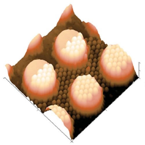
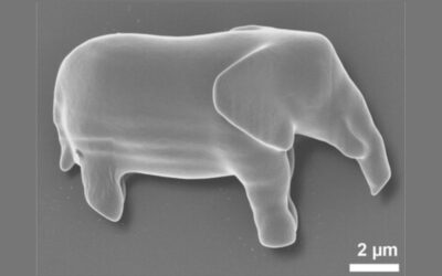
 Nanosized features can easily be printed accurately onto an already patterned surface, using a new technique called nanoimprinting by melt processing developed by US scientists.
Commercial production of devices based on nanotechnology demands that tiny, complex components be fabricated on a mass scale, at low cost, and in few steps. Nanoimprint lithography (NIL) is a common tool that can be used to fabricate nanostructures and devices that are 1/80,000 of the thickness of a hair. This technique presses a hard mold into a soft high-molecular-weight polymer film at high temperature and pressure to create nanostructures. However, if the polymer used is highly viscous (flows slowly), as such polymers often are, the NIL fails as the polymer does not spread properly. In particular, this makes it difficult to use NIL for printing nanostructures onto an already patterned microstructured surface. Use of lower molecular-weight polymers that are less viscous results only in the film becoming brittle and cracking, which renders it unusable.
To overcome this issue, scientists at the University of Central Florida, Stanford University, and the University of Arizona, USA, have developed a new technique called nanoimprinting by melt processing (NIMP) in which they use a mixture of a low-molecular-weight polymer and a plasticizer. The team, led by Professor Jayan Thomas, found that this composite could be used successfully at low temperatures and pressures, without the need for any expensive equipment. Their clever use of this mixture reduced both the viscosity of the polymer and the brittleness/cracking of the resultant film. The scientists have used their new technique to accurately print large-area nanopatterns with varied feature sizes over underlying topographies, including onto and near micropillars.
Thomas and his colleagues believe that NIMP has many benefits for making nanophotonic and nanoelectronic device structures at low cost; this should have a significant impact on both the ongoing research in this area as well as the possible commercialization of such devices. They believe that their technique will benefit much of science and technology by allowing the production of more versatile nanostructures.


