The incorporation of polymeric materials, including conjugated polymers, in various devices is a current trend since it can help to reduce both their weight and cost. Owing to the specific expectations for the next generation of microelectronic and optoelectronic devices, conjugated polymers have been widely studied since their conductive properties were discovered.
Polymeric conductors have been the subject of intensive studies that notably focused on their use as active layers or transparent electrodes in devices such as thin‐film organic field‐effect transistors (OFET). Among the available conjugated polymers, the commercially available poly(3,4‐ethylenedioxythiophene) (PEDOT) has been a candidate of choice.
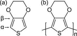
Chemical structures of (a) EDOT and (b) PEDOT.
In an attempt to increase the conductivity of plasma‐polymerized EDOT (ppEDOT) thin films, Nicolas D. Boscher and his team in Luxembourg investigated the AP‐PECVD reaction of EDOT in an ultra‐short square‐pulsed AP‐DBD for the first time.
The team researched several Ar/O2 plasma gas mixtures and demonstrated the occurrence of oxidative polymerization in an AP‐DBD process using ultraviolet‐visible spectroscopy (UV‐vis) and Raman spectroscopy. Finally, the morphology, transparency, and electrical properties of the ppEDOT thin films were characterized with the aim of understanding the potential and limitations of ultra‐short square‐pulsed DBD for the synthesis and deposition of conducting polymers.
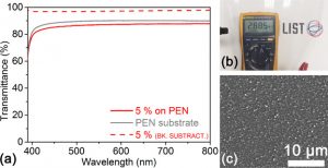
(a) Transmittance spectra of the ppEDOT thin film deposited on PEN using the Venturi nebulizer and a plasma gas containing 5% oxygen. Transmittance spectra of the PEN substrate is provided in gray. (b) and (c) show the optical image and scanning electron micrograph of the ppEDOT thin film deposited on a 23 × 15 cm2 PEN foil, respectively. The multimeter reading in picture (b) is ca. 3 MΩ across the length of approximately 25 cm
The team successfully achieved the deposition of durable and highly transparent conducting ppEDOT thin films at room‐temperature and atmospheric‐pressure using a scalable AP‐DBD process that does not involve the use of any halogen oxidant. The plasma gas composition and electrical excitation, as well as the monomer delivery rate and injection mode, were all shown to have an influence on the ppEDOT properties, namely transparency and conductivity. Read more about this study and more in the latest April issue of Plasma Processes and Polymers.