Dynamic random access memory (DRAM) is the most common type of memory found in modern computers, such as servers, laptops, and smartphones. A major challenge currently facing this technology is scaling of the capacitor (one of two components that make up the DRAM cell) as the technology node shrinks to <1 nm. The capacitor requires both high capacitance (low equivalent oxide thickness) and a low enough leakage current in order to function efficiently. However, as electrode size and dielectric thickness decrease, meeting these requirements becomes difficult. Accordingly, the development of dielectric materials with extremely high permittivity, such as SrTiO3 (STO), has attracted a great deal of attention
STO thin films have a permittivity of >150 when crystallized in the perovskite structure. Along with its high crystallinity, the low defect density and smooth interface/surface achieve a low leakage current. In their recent publication, Prof. Cheol Seong Hwang and coworkers developed a two-step growth process of STO thin film (seed and main layer) using an atomic layer deposition technique.
In this method, the seed layer is annealed by a rapid thermal annealing process before the main layer is grown on top. In this way, the STO main layer can be locally and epitaxially crystallized in situ on the STO seed layer without any post-deposition annealing. The in situ crystallization proved essential to restricting the generation of microcracks in the film, which act as leakage paths even under a small bias voltage.
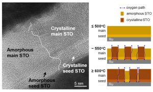
The effect of the annealing temperature of the seed layer on the STO-based capacitor was then investigated. Since the annealing process controlled the properties of the seed layer, which acted as the template of the main layer growth, it significantly affected the physical and electrical properties of the main layers. In addition, since the total thickness of the STO dielectric film was only ≈12 nm, the ≈4 nm thick seed layer played a significant role in determining the overall electrical performance of the film.
By careful experimental design it was revealed that 550 °C was the critical annealing temperature where both the seed and main layers began to crystallize. When the annealing temperature fell below 550 °C, the film remained in the amorphous phase, and when it rose as high as 600 °C, the STO seed and main layers were fully crystallized in the perovskite structure. Moreover, it was found that because of the columnar growth of STO films, the vertical grain boundaries in the crystallized films acted as oxygen diffusion pathways, which enhanced the growth rate of the main STO layer compared to the amorphous phase seed layer. Using 550 °C as the seed annealing temperature, the resulting STO film, which had a mixed phase of amorphous and crystalline seed regions, showed a surface “roughness” due to the difference in the growth rates of the two phases.
Consequently, 0.52 nm equivalent oxide thickness and 2.5 x 10⁻⁸ A cm-2 leakage current density were achieved through optimization. The results of this study are quite promising as they show the high potential of STO materials in creating the next generation of DRAM capacitors.
“This research provides a specific guideline to achieve high-performance SrTiO3-based capacitors, introducing the way for innovative next-generation DRAMs,” says Prof. Cheol Seong Hwang, the principle investigator of this study.
The researchers suggested that a novel capacitor structure made of SrRuO3/STO/SrRuO3 should be considered, where the perovskite-structured SrRuO3 electrode can act as a seed layer for the in situ crystallization of the STO film. In this way, the time-consuming two-step growth process of the STO dielectric layer would no longer be necessary as the electrode could serve as the crystallization template layer. The all-perovskite-structured capacitor may indeed be the future of DRAM.