Portable electronics, such as tablets or smartphones, have become multi-functional devices, and upcoming generations are predicted to include virtual and augmented reality applications and/or visualization features, like pico-projectors. For these applications to become a reality, the development of efficient, compact, low-cost, high power light sources in the infrared and in the visible red, blue, and green spectral regime are key technologies.
Superluminescent diodes (SLEDs) are optoelectronic semiconductor light sources with unique emitter characteristics that can fulfill these specifications. They combine laser-like beam properties with broadband emission (similar to LEDs), and provide high output power densities with short coherence length for visualization and sensing applications.
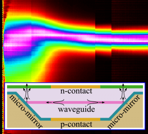
Cross-section of surface emitting micro-mirror SLED with its normalized spectral evolution.
However, SLEDS are commonly designed as edge emitters, the fabrication of which is similar to laser diodes, which is based on wafer cleaving and the subsequent coating of facets and requires the handling of individual stripes or bars. As a result, the elaborate fabrication of SLEDs has been one of their major drawbacks, hindering them from becoming more appealing to bigger market segments. Furthermore, it is critical to suppress lasing in SLEDs through the suppression of optical feedback at the mirrors. This is achieved by maximizing the light out-coupling and reducing feedback by designed losses. Consequently, this results in relatively low SLED efficiencies.
In a recent study, collaborators from OSRAM Opto Semiconductors and the University of Kassel have reported novel surface-emitting SLEDs, which have been inexpensively fabricated. The SLED waveguide is terminated by integrated micro-mirrors, which deflect in-plane guided optical modes via total internal reflection towards the chip surface. In combination with thin film technology, where the wafer is flipped and bonded onto a new carrier and the substrate gets removed, the mirrors in such SLEDs are fabricated by a conventional dry etching process on wafer-scale. All other processing steps, including out-coupling surface treatments and final testing, are also done on wafer level, similar to thin film LED production.
The investigated devices emit at a peak wavelength of 950 nm with a spectral width of 10 nm. In superluminescence regime the observed output power is higher than 250 mW and the wall-plug efficiency exceeds 15%. Moreover, as the new surface emitting approach allows the emission of light out of both waveguide ends, the achieved light out-coupling and wall-plug efficiencies of these demonstrator devices are already comparable to their edge-emitting counterparts.