Harnessing light on the nanoscale has enabled ground-breaking technological developments, from enhanced biosensors to solar cells and quantum computers.
This is achieved by manipulation of light waves through light–matter interactions using materials that are patterned with nano-meter-scale objects, smaller than the wavelength of the incoming light. Light can therefore be manipulated through specific patterns and arrangements on the material’s surface to control its direction, convert it to an electrical signal, scatter, or absorb it.
Organic–inorganic perovskites are a promising class of materials for advanced optoelectronic applications and are emerging as an alternative to conventional semiconducting materials in solar photovoltaic technologies.
Perovskites were first discovered in 1839, when German scientist Gustav Rose discovered a new calcium titanate-based material in the Ural Mountains, and named it “perovskite” in honor of the Russian mineralogist Lev von Perovski. Over the next century, research in this area would explore new combinations of elements to harness the material’s unique properties for a range of commercial applications.
Metal‐halide hybrid perovskites (MAPbX3, where X = [I, Br, Cl] and MA = CH3NH3) in particular are up-and-coming in solar energy, though a limitation in their widespread use and further development is their instability during conventional nano-processing techniques, such as electron beam lithography. Here, an electron beam is used to write custom shapes onto a surface by essentially melting specific areas of the solid surface and washing the excess material away with solvent. Perovskites, unfortunately, degrade under the electron beam and in the presence of some solvents and high temperatures, making this and other similar manufacturing techniques impossible.
Therefore, a completely new approach for this class of materials is needed to enhance their desirable properties (i.e., light manipulation) without damaging it during processing. In a recent study published in Small, a collaborative team of scientists has developed a unique technology for non‐destructive nanopatterning of organic–inorganic metal‐halide perovskite films.
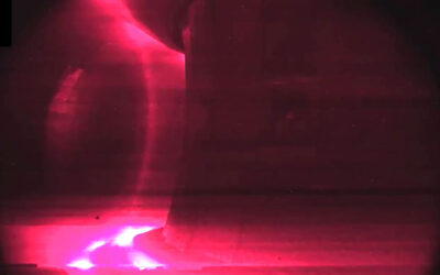
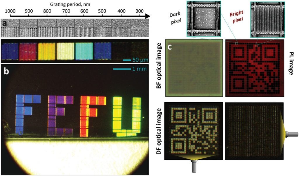
Compared to conventional semiconductors, perovskite has poor thermal conductivity, which makes laser processing suitable for creating precise, small patterns. In a normal semiconductor with high thermal conductivity, the heat will be scattered in all directions and the desired thin, sharp edges of the nanopattern become distorted. Given perovskite’s thermal resistance, the researchers were able to construct an array of nanophotonic designs using short laser pulses to evaporate the material’s organic element at a relatively low temperature, creating functional and high quality nanoelements while minimizing degradation.
“The achieved fabrication quality is comparable with previously reported expensive lithography‐based techniques, while also providing high reproducibility, productivity, and flexibilty regarding the range of possible designs,” said the authors in their study.
The technique also allows for thinning of the perovskites by careful removal of material layers, which the team hopes will pave the way to more complicated 3D architectures.
The team went on the demonstrate the application of their new technique in color marking, non‐destructive printing of nanowire‐based lasers, as well as delicate solar cell scribing. They also demonstrated proof-of-concept for large‐scale encryption of optical information for optical computers, which use photons to carry out computation.
Reference: A. Y. Zhizhchenko, et al., ‘Light‐Emitting Nanophotonic Designs Enabled by Ultrafast Laser Processing of Halide Perovskites.’ Small (2020). DOI: 10.1002/smll.202000410