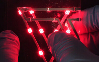
Scientists in the USA have shown how to exploit all three dimensions of patterned photoresists rather than just the usual two, to make complex components using just one template.
Patterning surfaces is big business, as it can be used to make many components for computer chips such as transistors, resistors, capacitors, etc. The race is on to make smaller and more efficient, faster computers, and materials scientists are making the first steps in this race. Lithography is usually the method of choice to make such components. The fabrication can be a tedious process as each component needs to be drawn separately onto the surface using an appropriate template mask. To make a whole functional component many lithographic steps are needed.
The group of George Whitesides at Harvard University, USA, has devised a process to create many different shapes on a surface, all using a single mask. They make use of a known process called shadow evaporation, in which the “shadow” cast by a feature on a mask controls the pattern on the surface. Think of a stencil held over a flat surface; if you spray paint from directly overhead then you will end up with a pattern on the surface just like that of the stencil. By changing the angle at which the paint is sprayed through the stencil, you can alter the pattern obtained with the same stencil. Usually this effect is undesirable when painting but it works for Whitesides and his team. Although shadow evaporation has previously been used to make small shapes, it normally still involves many steps to produce a component. Whitesides’ team have gone one better and produced functional and interconnected layered systems using their new, quicker technique which they call topographically encoded microlithography (TEMIL).
The pattern finally produced on the surface using TEMIL is defined by the 3D shape of the photoresist mask used, as well as by the position and angle of the surface in relation to the photoresist. Exploiting 3D rather than flat 2D masks allows them to create a greater range of shapes on the surface, so the team can use one 3D mask and several deposition steps with a single directed beam at differing angles to make complicated layered structures; much simpler than having to use a different mask for each step. The reduced number of steps should mean the final chips should become cheaper.
The team have already made a transistor, an AND gate, a capacitor, and a wire in arrays of several thousand using TEMIL. They believe that it can be used to make many different components and could be particularly useful on softer substrates such as those used in flexible electronics. Maybe one day TEMIL could be used to make complete computer chips on soft surfaces!


