The Advanced journal brand is known internationally for the publication of cutting-edge, high-quality scientific research. Beautiful covers from across the journal family adorn offices and conference presentations everywhere, as well as the occasional t-shirt or mug. As Advanced Materials is celebrating its thirtieth birthday, I decided to dig into the archives to take a look at some of the creative, interesting and important work that we’ve published over the years. For example…
The very first all-organic electronic device displaying the same characteristics as silicon-based devices was reported in Advanced Materials in 1990. “Recently,” wrote the authors, “an interesting step has been made by the study of a new class of well-defined and easily processable organic semiconductors, formed by conjugated oligomers.” The report from Francis Garnier et al., which remains popular today (eight citations so far from papers published in 2018, according to the Web of Science), described the fabrication of a soft and flexible thin-film transistor from all-organic materials that offered higher carrier mobilities and better performance than devices using the standard amorphous silicon insulator. Due to their molecular nature, organic semiconductors were “expected to be much less sensitive to external impurities”, meaning that they did not “require a controlled atmosphere and drastic purity conditions”. “A very promising field is thus opening for organics,” the authors correctly predicted: the field of organic electronics continues to flourish, gracing the Advanced journals most recently with reports on the control of interfacial self-doping in organic electronics and molecular-scale simulations for organic electronic devices.
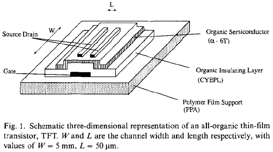
The first all-organic electronic device displaying the same characteristics as silicon-based devices was published in AM.
In 1997, a paper appeared which offered a solution to one of the biggest challenges in carbon nanotube production. “Carbon nanotubes are typically produced by arc discharge,” informed Jean-Marc Bonard et al., “with a wide distribution of lengths, helicities of the layers, and diameters.” Their technique, reported in Advanced Materials, offered the nondestructive size selection of carbon nanotubes by applying sodium dodecyl sulfate (SDS) as a stabilizer: “no sedimentation occurred, indicating the required metastability to start a purification process.” That process was the filtration of their colloidal suspension to remove the smaller nanoparticles, separating out the desired nanotubes with the help of sonication. “The best results were obtained with 0.4 µm pores and strong sonication,” they observed. They also experimented with just leaving the SDS-supported suspension to rest, letting the larger aggregates settle while the smaller particles remained dispersed (controlled flocculation), and linked the length of the tubes collected to the concentration of SDS in the solution. The refining of such methods is still under consideration, including the greener processing of carbon nanomaterials.
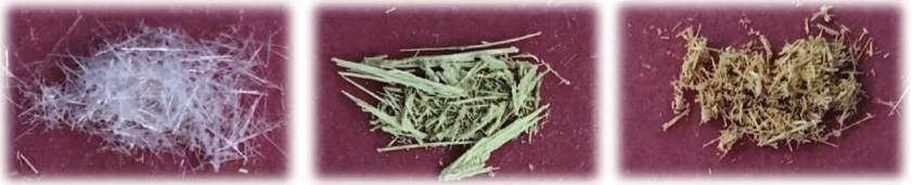
Centimeter-long needles of carbon nitride, inspired by a review from 2003.
Skipping forward to March of 2003 brings us to a review of one-dimensional nanomaterials, the most highly cited Advanced Materials paper of all time – so far – with over 7000 citations, at least 150 of which are from this year alone (according to Clarivate’s Web of Science). The review collated information on wires, rods, belts, and tubes, focusing on the chemical synthesis methods for their anisotropic growth. “The ability to generate such minuscule structures is essential to much of modern science and technology,” wrote Younan Xia et al., who also examined the unique properties of such structures, including “size-dependent excitation or emission, quantized (or ballistic) conductance, [Coulomb blockade], and metal–insulator transition.” They neatly summarized the importance of their paper and the key to its ongoing popularity: “It is generally accepted that quantum confinement of electrons by the potential wells of nanometer-sized structures may provide one of the most powerful (and yet versatile) means to control the electrical, optical, magnetic, and thermoelectric properties of a solid-state functional material.” Current research on 1D materials has produced centimeter-long needles of carbon nitride and nanomachines for biochemical delivery and sensing.
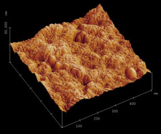
AFM tapping-mode image of the material used to create the record 5% PCE polymer solar cells.
A little further ahead in 2005, an Advanced Functional Materials paper on bulk heterojunction polymer solar cells by Alan J. Heeger and co-workers proposed “specific fabrication conditions” to reach device efficiencies approaching 5%. Their process used P3HT:PCBM and included a post-production annealing step at 150 degrees Celcius, which formed “thermally stable nanoscale, interpenetrating donor–acceptor networks” and led to higher polymer crystallinity and improved contact with the electrode. “Devices annealed at high temperature during fabrication,” wrote the authors, “are expected to be even more stable under ambient conditions”. Their record efficiency was attributed to a reduced series resistance due to enhanced charge generation and transport. The report has been cited around 3800 times, most recently by works on organic solar cell carrier dynamics, a graphene interface in stacked P3HT systems, and stretchable semiconductors for plastic electronics.
In 2008, Georgia Tech’s Zhong Lin Wang gave us some insights into the future of certain nanosystems and their energy generation mechanisms with a Feature Article in Advanced Functional Materials. He made the salient point that the size of a battery “largely dictates the size of the entire system”, defining a critical limitation for the miniaturization of powered devices of any sort. Unfortunately, smaller batteries have shorter working lifetimes, so the solution he described lay in the development of wireless, self-powered systems instead. “The goal of nanotechnology,” wrote Wang, “is to build self-powered nanosystems that are ultra-small in size, and exhibit super sensitivity, extraordinary multifunctionality, and extremely low power consumption. The resultant energy harvested from the environment should be sufficient to power the system.” His paper focused on nanowire-based systems with a view to creating implantable devices capable of harvesting energy directly from the human body; ten years on, Professor Wang has demonstrated the use of triboelectric nanogenerators for everything from harvesting wave energy in water to acceleration/vibration sensors.
A short step forward to 2010 brings us to an Advanced Materials review by Rodney S. Ruoff and co-workers, then at the University of Texas at Austin, focused on a popular little material called graphene. “Graphene is an exciting material,” the authors wrote, which is well validated by the paper’s 4000+ citations (including many patents). After describing its synthesis, properties, and applications – as well as those of chemically modified graphene and graphite oxide – they summarized by suggesting that “CVD growth on metal foils has exceptional potential for, ultimately, the production of endless lengths of [graphene] of desired widths (‘graphene foil’) that could then be picked up by roll-to-roll processing” if only finer control over the number of layers could be achieved. Alternatively, they proposed that chemical processing routes “may be able to produce fairly large amounts of ‘graphene’ cost effectively; however, the chemical details… need to be more fully understood.”
Wei Luo of Tongji University and Liangbing Hu of the University of Maryland are two authors who used the Ruoff review as a source of inspiration for their recent work ‘Highly Conductive, Light Weight, Robust, Corrosion-Resistant, Scalable, All-Fiber Based Current Collectors for Aqueous Acidic Batteries’, published in Advanced Energy Materials. “We cited this ‘old’ review since it is still relevant to our own study,” say the researchers. “Many ideas can still be generated based on [this] review.”
Professor Guihua Yu of the University of Texas at Austin would agree, having cited this work in his own Advanced Materials paper, ‘Structural Engineering of 2D Nanomaterials for Energy Storage and Catalysis’. “The review article by Ruoff and co-workers is a truly classical one,” he says. “The comprehensive overview on graphene and graphene oxides materials covers from their controlled synthesis and functionalization, to the resulting novel properties and significant effects on technological applications. The fundamental insights present in this review still translate well to the continuous discovery of new candidate 2D materials and rational structural control and tuning of the growing family of 2D nanomaterials for many energy-related technologies.”
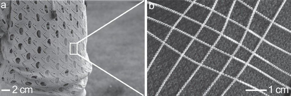
Flexible energy-harvesting fibers mean wearable solar cells to power small electronics.
Another very active area of research is the integration of energy-harvesting systems into wearable devices and, a few years back in 2014, it motivated the fabrication of a polymer solar cell fiber that could be woven into textiles. The article in Small from Fudan’s Huisheng Peng and co-workers described flexible and stretchable solar cells made from coiled titanium wires onto which titania nanotubes, P3HT:PCBM, PEDOT:PSS and, finally, multiwalled carbon nanotube sheets were layered. The coils were threaded with elastic fibers and woven directly into textiles used to produce clothing. “Importantly,” wrote the authors, “the produced voltage is continuously enhanced with more 1D PSCs that are arranged in series, so they can be effectively scaled up for various practical applications.” The Peng group is still heavily researching such flexible energy systems, including fiber-shaped batteries, a system which converts potential energy from the water–carbon interface into electrical energy to power small personal devices, and dynamic textile-based display systems capable of interfacing with a mouse brain.
And now it’s time for me to close the archives and get back to our submissions inboxes – the next set of exciting discoveries awaits.
Featured Image Credit: Fred Bigio via Flickr, CC-BY 2.0