WSe2 is a two-dimensional material that behaves as a semiconductor. This material system is particularly attractive for possessing: i) ideal properties to make electrical devices such as field-effect transistors, and ii) optoelectronic properties compatible for efficient light-emitting devices. If this material is confined to a single dimension in the form of a so-called nanoribbon or nanowire, unique material properties are expected to emerge.
In a recently published article in Small Methods, a chemically assisted focused-helium-ion-beam-induced etching process is introduced by a team of researchers from the University of Tennessee and Oak Ridge National Laboratory, TN, USA, led by Dr Philip Rack. This process enables the patterning of WSe2 on the nanoscale.
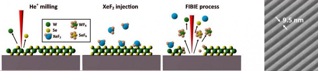
a–c) Schematics of an He+ milling process (a), XeF2 gas injection (b), and focused-ion-beam-induced etching of WSe2 (c). d) SEM image of WSe2 nanoribbons created with the FIBIE process. More information here.
The etching process utilizes a chemical reaction for rapid material removal and enables high-resolution patterning of WSe2 with a 5× enhanced material removal rate relative to standard ion bombardment alone. This enables the formation of WSe2 nanoribbons with dimensions less than 10 nm due to the extremely high resolution of the helium-ion microscope. The direct-write nature of the etching process enables the formation of highly aligned nanoribbons, which can be utilized for advanced electronic and optoelectronic device fabrication.
The WSe2 nanoribbons demonstrate interesting optical properties, and nanoribbon electrical measurements are reported for the first time. This direct-write etching process provides a simple method for preparing 1D nanoribbons out of WSe2 and other transition-metal dichalcogenides (TMDs). Many simulation studies have detailed the interesting properties that 1D TMDs should exhibit. This etching process and future advanced processes will enable the experimental study of interesting physics that arise due to quantum-confinement effects when TMDs are confined to one dimension.
Ultimately, direct-write nanoprocessing techniques like this one detailed by Dr Rack and his team provides tools for the rapid exploration of advanced devices.