A novel ultra-black broadband absorber concept based on a needle-like silicon nanostructure has been developed: ultra-black silicon (ub-Si) exhibits an absorptance of more than 99.5% between 350 nm and 2000 nm and about 99.8% between 1000 nm and 1250 nm.
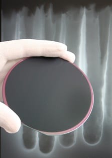
Ultra-black silicon absorber
From solar thermal energy conversion over optical spectroscopy to photothermal light detection – these and many more applications need highly efficient light absorbers. Materials with broadband absorptance as high as possible are top of the list of desirable materials. From that point of view, there are three interesting materials with broadband absorptance of more than 99%: gold-black coatings, large area carbon nanotube arrays (CNT) and the so-called ultra-black nickel-phosphorus (ub-NiP). Although CNT exhibit the highest absorptance of more than 99.9% around 550 nm, the mostly used material is ub-NiP because of its well established, simple fabrication and its absorptance of up to ∼99.8%. Martin Steglich and his colleagues from Friedrich Schiller University Jena (Germany) now add an attractive absorber concept based on needle-like silicon nanostructures called Black Silicon.
The novel absorber material consists of a 1.6 μm deep Black Silicon nanostructure established on a highly doped silicon substrate by inductively coupled plasma reactive ion etching (ICP-RIE) and an additional dielectric coating (Al2O3) prepared by atomic layer deposition. The fabrication procedure is free of lithography and only consists of a dry etching and an oxide deposition step. The etching relies on a randomly distributed formation of silicon oxyfluoride particles (SiOxFy) on the silicon surface. The new method is reliable, well-repeatable, up-scalable and does not require lithography or any sample pre-treatment. Fabrication of the absorbers is consistent with CMOS standards.
The absorber concept with Black Silicon yields an absorptance beyond 99% in a broad wavelength range between 350 nm and 2250 nm. Particularly and in contrast to other publications, the high absorptance in the wavelength region beyond the silicon bandgap (λ > 1100 nm) is accomplished by applying highly doped, degenerate silicon substrates which exhibit a finite coefficient of light absorption in this range. To stay consistent with the term ultra-black NiP, the concept is similarly referred to as ultra-black silicon (ub-Si).
Improved absorbers also incorporate an additional oxide capping layer on the nanostructures and reach an absorptance of A > 99.5% in the range of 350 to 2000 nm and A ∼ 99.8% between 1000 and 1250 nm.