High-speed electronic devices, such as transistors and light-emitting diodes, are used in many different fields, including communications, infrared remote sensing, and optical detection. However, their performance can be limited when electrically active defects occur at the interface between the substrate material and the metal oxide material.
In a communication in Advanced Materials, Xing Wu, Litao Sun, Kinleong Pey, and co-workers from East China Normal University, Southeast University, and Peking University in China; The Aerospace Corporation in USA; and Singapore University of Technology and Design in Singapore use in-situ transmission electron microscopy (TEM) to record the dynamic evolution of structural and electrical interfacial properties of zirconium dioxide (ZrO2) films on aluminum oxide (Al2O3) and indium gallium arsenide (InGaAs) substrates.
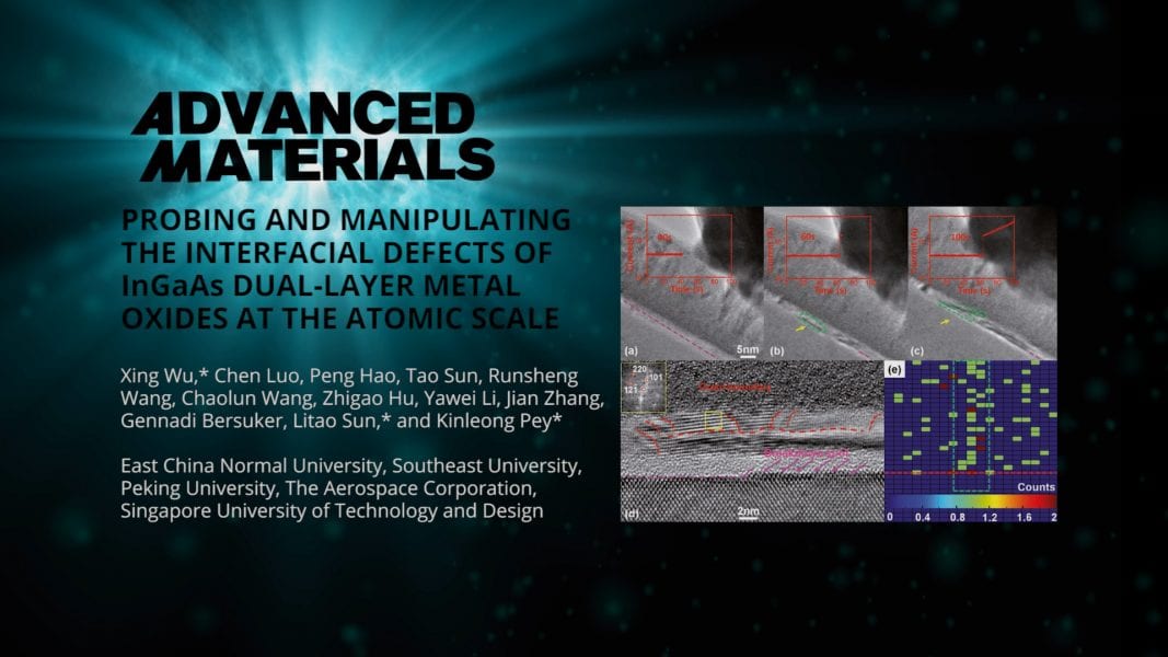
A specially designed focused ion beam technique is used to fabricate a TEM lamella containing many individual nanodevices consisting of ZrO2/Al2O3/InGaAs, each with a thickness of ≈50 nm and a width of <20 nm. This one-cut, many-device technique improves the efficiency of the experiments. The multidevice specimen is analyzed using in situ TEM, while stress-induced leakage current measurements are taken to characterize microstructural defects.
Initially, the interface between the TiN/ZrO2 and ZrO2/Al2O3 are defect-free, and the leakage current density is low. However, as a positive sweep voltage from 0 to 3 V is applied, the current increases abruptly at 2.6 V by one order of magnitude and defects can be seen in the ZrO2 layer. To probe the source of defect generation, a constant stressing voltage of 1.9 V is applied to the devices. At ≈60 s, the gate current rises by one order of magnitude and is accompanied by vertical and horizontal expansion of defects in the ZrO2 layer. Spectroscopic methods show that atomic-scale structural changes are primarily caused by O-atom vacancies. Electron energy loss spectroscopy mapping and simulated defect and heat profiling show that these vacancies, and therefore defects, originate at the ZrO2/Al2O3 interface before propagating into the ZrO2 layer.
To find out more, please visit the Advanced Materials homepage.


