 Dr. John Uhlrich, Editor-in-Chief of Energy Technology, talks to Professor Subodh Mhaisalkar of Nanyang Technological University, Singapore about his recent article on fully printable perovskite solar cells, which brings new insights towards the understanding of perovskite solar cells and their large-scale commercialization. It is also included in a pair of dual Special Issues on Perovskite Optoelectronics, for which Prof. Mhaisalkar acted as co-guest editor.
- Could you briefly explain the focus and findings of your article to a non-specialist and why they are of current interest?
In a short span of less than years, metal-halide-based perovskite solar cells have exceeded solar conversion efficiencies of 22%. With methyl ammonium lead halide, CH3NH3PbI3, as the primary semiconductor of interest, perovskites represent the highest efficiency solution-processed solar cells and are well-positioned to complement and/or challenge silicon solar cells. One of the key barriers for industrialization includes reliability, and cells that use carbon for passivation and charge transport are arguably the most promising in the short term to deliver solar cells that deliver reliability in excess of 15 years. This work represents a key step in improving the stability and performance of these carbon-based perovskite solar cells.
- Could you please explain the motivation behind the study?
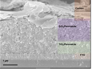
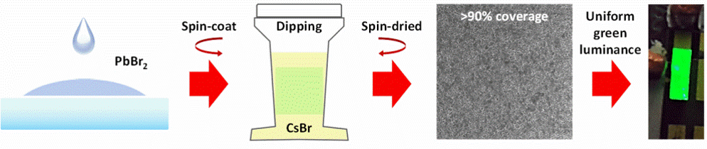
Perovskite solar-cells have reached record values of 22.1%. These champion cells are however typically less than 0.1 sq cm in size, employ hole transport materials (HTM) such as spiro-OMeTAD with gold electrodes, and do not show promising stability upon light, moisture, and heat exposure. The motivation of our study is to deliver solar tiles that would exceed 30 cm x 30 cm in size, would be fully printed, and would be able to meet most of the reliability requirements that silicon solar cell modules are expected to meet. Although metal-halide perovskites are known to deliver highly crystalline films with long-range charge transport, their defect densities are under increased scrutiny as they are viewed to be barriers to both increased efficiencies as well as improved stabilities. Small amounts of excess of PbI2 in the perovskite layer have been demonstrated to improve the power conversion efficiencies, with device architecture containing spiro-OMeTAD-Au. The addition of excess PbI2 is thought to promote the crystallization process and to have a passivation effect at the interfaces, thereby resulting in reduced recombination rates. The purpose of this study was thus to find a facile method to improve the crystallization of the perovskites and to passivate the interfaces so as to improve both performance and stability of these carbon-based devices.
- How long did this investigation take?
The investigation included a selection of the materials involved, process optimization, device physics examination, a study of the charge dynamics, and finally reviewing the stability under moisture, temperature, and illumination stresses. The study also represented a partnership between materials, physics, and device engineering groups, and took close to one year to be completed.
- This work contains well-controlled, fundamental characterization of photovoltaic devices in a laboratory setting, but with very practical implications. How do these results contribute to the realization of practical perovskite photovoltaic devices? What was the most difficult part about completing this study? Did anything surprise you about your findings? How will you follow up on this work?
Realization of solar cells that are viable for industrialization is only possible through a very detailed analysis of the materials, processes, device architecture, and charge transport that enable the electrons and holes to be collected at the selective contacts. These results address one of the many steps that are essential before we can exploit the potential of these exceptional semiconducting materials in practical applications such as solar cells. The key aspect we pursued in this work was to study only one variable at a time, that is, PbI2 addition and its defect passivation, and to understand its impact on device scaling and performance. The main surprise was that although we could improve the open circuit voltage, the presence of Pb arguably compromised the device stability. The main learning was to devise other methodologies that would yield the same result. We are following up on this work by using multi-cation systems and other methodologies for defect passivation using iodides and other halides.
- These works were published as contributions to dual Special Issues of Energy Technology and ChemSusChem on “Perovskite Optoelectronics”, which you co-guest edited with the organizers of the symposium on this topic at the ICMAT-2017 in Singapore. Towards realizing perovskite photovoltaics on a practical scale, what are some of the other most important areas for future development? Have some of these also been addressed in the Special Issues?
Our findings to date support the notion that carbon-based devices are likely to be the first minimum viable product for market entry in photovoltaic devices. The potential for solar tiles, utility solar, and also building integrated photovoltaics (BIPV) based on these perovskites is very promising and several companies have defined roadmaps to realize this over the next 2-3 years. For the longer-term and wider applications, it is essential to replace the archetypical CH3NH3PbI3, with more stable perovskite formulations, introduction of layered perovskites for passivation and stability, and replacing the carbon electrode with inorganic electrodes that will yield both transparency and stability. Transparent electrodes will also open up the possibility of combining perovskites with silicon solar cells in a tandem configuration, where the former would harvest more of the UV and visible parts of the spectrum and the latter would harvest the IR spectrum, thus improving the efficiencies of silicon solar modules.
- One of your other contributions to the Energy Technology Special Issue reports an interesting advance on perovskite light emitting diodes. How close are perovskites to realizing application in this field, and is this leading or trailing the application of such materials in photovoltaics. Is there overlap between these two fields? Can an advance in one lead to an advance in the other?
It has been recognized that one of the key performance metrics of high-quality semiconducting materials is its photoluminescence. Like the best-in-class semiconductor for light emission, GaAs, perovskites have demonstrated excellent properties for both solar cells, light-emitting diodes (LEDs), and lasers. Light emission was first demonstrated in perovskites in 2014; however since then there have been multiple reports where perovskite LEDs (PeLEDs) have equaled or exceeded the properties of organic light-emitting diodes (OLEDs) or quantum dot light-emitting diodes (QLEDs). These include luminance higher than 91,000 cd/m2 and current and quantum efficiencies approaching 60 cd/A and 14%, respectively. Very promising progress has been observed in PeLEDs and new materials and approaches are emerging that hold the promise to approach all of the milestone efficiencies of OLEDs and QLEDs within the next 2-3 years.
Light harvesting in solar cells and light emission in LEDs are very closely related, and in particular new active materials, electrodes, defect passivation, and stability issues are very similar in both devices. Undoubtedly, they are two faces of the same coin and progress in either field will translate readily to the other. Furthermore, the development of both solar cells and LEDs has also propelled perovskites into adjacent fields that include spintronics, photostriction, laser cooling, photodetectors, and long-wavelength radiation detection, among others.