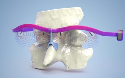
Circuits and electrodes that curve through three-dimensional space are finding applications in antennas, display devices, and image sensors. However, problems with the fabrication process for these devices limit the shapes that can be created.
In Advanced Functional Materials, Heung Cho Ko and co-workers from Gwangju Institute of Science and Technology describe a novel process for reliably fabricating three-dimensional electronic devices.
Hun Soo Jang, a researcher on the project, states:
“We made these devices over a number of steps. Firstly, an electronic element was transferred onto the surface of a specially designed polymer called acrylonitrile-butadiene-styrene (or ABS). This was then laminated, sealing the device.”
Seonggwang Yoo, another member of the research team, further describes the process:
“We then printed a series of lines onto the ABS layer. These lines introduced stress points into the design. When heated, these stress points caused the material to bend in a predicable manner.”
If the electronic devices were bent manually, the metal or silica inside would crack. However, using the heating process enabled by this novel design, no cracking could be detected.
Using these lines, it was possible to fabricate a wide range of complex shapes—from a razor and a basket to a standing wave.
To learn more about the fabrication process for these three-dimensional circuits and electrodes, please visit the Advanced Functional Materials homepage.