Organic–inorganic hybrid perovskites have tremendous potential for next‐generation electronic and optoelectronic devices due to their remarkable carrier dynamics. Hybrid halide perovskites; however, are known to be very sensitive to trace amounts of water, and are therefore not compatible with standard microfabrication techniques.
Previous studies in the literature have mostly been based on polycrystalline forms of perovskites. For single crystals, Van Der Waals epitaxial growth on pre-patterned wafers has been demonstrated with low yield and poor reproducibility of randomly oriented large crystals.
Researchers have demonstrated for the first time a robust and efficient protocol involving microfabrication that enables the integration of an emerging class of materials into modern electronic devices, which is a pivotal step for real applications and large-scale production.
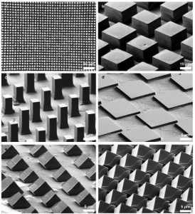
SEM images showing the controllable homoepitaxial growth of organic–inorganic hybrid perovskites.
The direct photolithography problem was first solved by using a layer of polymer to repel water and other solvents that are widely used in photolithography, and degrade halide perovskite materials.
A method that allows controllable growth of single crystalline halide perovskites with various morphologies, growth direction and thickness was developed.
The result is a novel method to pattern and control the growth of single crystals of hybrid perovskite on the micro/nanoscale. It is single crystal that promises better electronic and optoelectronic properties than polycrystals. The crystals with controllable morphologies, orientations, and sizes are critical building blocks for a range of functional devices. This method provides a universal strategy for a variety of halide perovskite materials.
Theoretical research points to single crystal perovskites that have lower trap density, longer diffusion length, higher mobility and better stability comparing with polycrystalline. Together with the grain boundary free property, single crystal perovskite-based devices such as solar cells, LEDs, and photodetectors are believed to be able to perform much better. However, integrating single crystals in electronic devices has been stagnant in the literature for a long-time due to the uncontrolled bulk size of these materials.
This research however introduces an easy and efficient method to control the perovskite single crystals into micro/nano scale, which unlocks the potential of these materials in electronic devices.
The next challenge is to scale-up the production of this process from benchtop demonstrations to large volume manufacturing.