Ultrafast electron microscopy (UEM), pioneered by the Nobel Laureate Prof. Ahmed Zeweil of the California Institute of Technology, provides an unprecedented means of interrogating ultrafast physical and chemical processes with ultrahigh spatial and temporal resolution at the challenging angstrom and attosecond scales.
This technique, however, has stringent requirements on the quality of the probing electron beam. In compromising the narrow energy spread, current state-of-the-art UEMs employ optically-driven sources, which afford simple, yet comparatively poor temporal resolution.
Prof. Qing Dai and his team of the National Center for Nanoscience and Technology, China, alongside collaborators from Peking University, Zhejiang Normal University, and Aalto University, have successfully demonstrated exciting findings on the realization of field-driven ultrafast photoelectron emission in a system capable of much higher phase synchronization than its photon-driven counterpart.
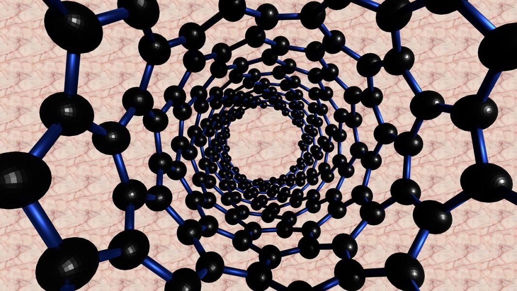
Using carbon nanotubes (CNTs), energy spreads as low as 0.25 eV have been achieved for the first time. This leading performance has been realized through optical sub-cycle electron tunneling excited by the shortest optical wavelength to date, only made possible through the team’s unique expertise in nanoengineering and their structuring of unique CNT surfaces. These nanosurfaces afford high field enhancement and high structural stability, and have potential as a new generation of ultrafast electron sources in microscopy and spectroscopy.
Prof. Qing Dai commented, “our results are of significant importance, both scientifically and technologically, towards the next generation of attosecond science and light-wave electronics research.”
This study is the first demonstration of its kind on field-driven ultrafast photoemission from self-assembled nanostructures. The CNTs used enable the production of highly coherent, low energy spread electron sources that are improved by at least one order of magnitude over incumbent state-of-the-art optical field-driven ultrafast electron sources, and twice improved over current photon-driven sources.
The team couple their skills of material manipulation at the atomic scale to allow them to exploit, for the first time, photoemission at a wavelength of only 410 nm—a readily-accessible and comparatively inexpensive optical window that has yet to be exploited with traditional metallic microstructures.
The researchers are confident that field-driven photoemission at even shorter pump wavelengths is likely in the near future. They believe this will reshape our understanding of strong field physics, and may lead the way to entirely new types of electron emission systems.


