Researchers at Georgia Institute of Technology have demonstrated the use of artificial intelligence (AI) in obtaining valuable insights to the operation of photonic nanostructures, which manipulate light for applications such as signal processing, communications, and computing. The study was recently published in the journal Advanced Intelligent Systems.
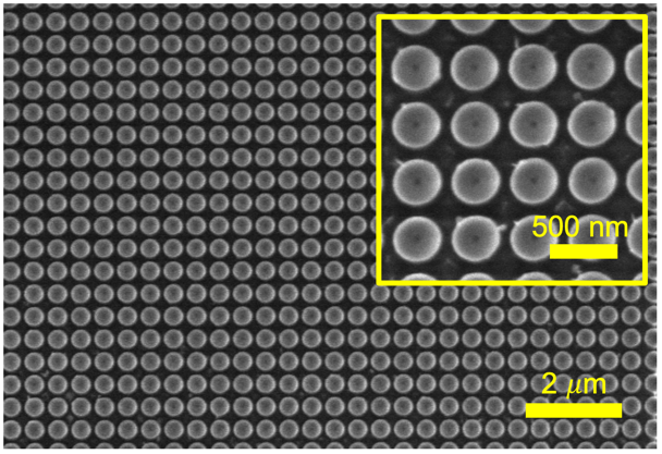
When light passes through these nanostructures, the collective effect of many nanoelements (i.e., inclusions with dimensions on the order of a few hundreds of nanometers) results in major changes in the spectral, spatial, and/or temporal properties of light. By proper selection of the geometrical features of these nanoelements, a large range of system-level functionalities (e.g., filtering, lensing, frequency conversion) can be achieved.
While most reports on using AI techniques in the field of nanophotonics are focused on the design and optimization of nanostructures, such as finding the geometrical features of meta-atoms, the new approach seeks to use the “intelligence” aspects of AI to understand the physics of these nanostructures, for example, in assessing the feasibility of a response from a given nanostructure.
This new approach is implemented in two steps: in the first step, the relation between input and output of the nanostructure is highly simplified by dimensionality reduction. By using an algorithm called “autoencoder,” the information of the nanostructure response is condensed from 100–200 variables into 2–3 variables, which facilitates the visualization.
In the next step, the responses from a large set of nanostructures with randomly selected geometrical features are used in the reduced-dimensionality space (also called the latent space) to find a convex enclosure (called a convex-hull) in the latent space that encompasses all feasible responses form the given class of nanostructure with a small error. The feasibility of any desired response from that class of nanostructures is likely if that response corresponds to a point inside the convex-hull in the latent space.
A more sophisticated algorithm called one-class support-vector machine (SVM) can also be used to provide different levels of confidence about the feasibility of a given response. “Using convex-hull or one-class SVM for assessing the feasibility of a given response from a selected class of nanostructures before attempting the computationally intensive design process saves a lot of time and avoids converging to a non-optimal design,” said Yashar Kiarashinejad, a Ph.D. student at Georgia Institute of Technology and one of the researchers working on this project.
A key aspect of this technique is training the different parts of the algorithm. This is done by simulating a few 1000 randomly designed nanostructures using commercial software. “By using an iterative approach, we can optimize the training process while trading accuracy with computation time,” said Mohammadreza Zandehshahvar, Ph.D. student and co-author of the study.
The trained algorithm will be tested with unseen feasible and unfeasible responses to ensure the desired accuracy before being used to assess the feasibility of any response.
The team expanded the capability of their approach by studying the convex-hulls and one-class SVMs of structures with different levels of complexity to show the possibility of using this technique to simplify the design of a nanostructure to achieve the same response. “We usually use our utmost fabrication capability to select a structure for a given response. This results in overly complex structures. Our approach can be used to simplify the design,” said Sajjad Abdollahramezani, another of the study’s contributors.
The approach also provides insights into the feasibility of a response from a given nanostructure. “This can serve as a guideline for changing the structure to enable an originally unfeasible response or make a more stable design against environmental or fabrication-induced changes,” said Omid Hemmatyar, one of the study’s co-authors.
The technique can be extended further to obtain far more information about the physical mechanisms for interaction of light with photonic nanostructures and form new classes of nanostructures to enable functionalities beyond the state of the art.
“What we see is just the tip of an iceberg. Using the information in the latent space can enable to learn the key features of the nanostructures in forming different classes of responses and evolving a starting nanostructure to a much more functional one for a desired application,” said Ali Adibi, the principal investigator and professor in the School of Electrical and Computer Engineering at Georgia Tech.
Kindly contributed by the authors