:All-Inorganic Hetero-Structured Perovskite Light-Emitting Diodes with High Current Density")
Pursuing novel new materials for fabricating efficient electrically pumped (lasing diodes) LDs with tunable emission wavelength has been the dream of numerous researchers across the globefor decades. However, conventional semiconductor materials that have been developed so far have certain drawbacks, such as the low carrier mobility in organic semiconductors, and rigid preparation techniques for inorganic semiconductors. Therefore, it is imperative to develop new semiconductor materials with nontoxic elements and high photoluminescence quantum efficiency and optical gain to achieve electrically pumped lasers.

Recently, hybrid metal halide perovskites have been the bright star for photovoltaic applications with high certified power conversion efficiency. More importantly, these perovskites possess considerably attractive optoelectronic properties, such as high photoluminescence quantum yield, high optical gain, and high carrier mobility. These characteristics make Sn-based perovskites the most appropriate candidate for electrically pumped LDs.
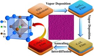
To achieve LDs with Sn-based perovskites, two obstacles need to be overcome. Firstly, smooth and full coverage cesium tin halide perovskite (CsSnX3) films with high quality are desirable, which is a prerequisite for amplified spontaneous emission (ASE) with low threshold; secondly, all-inorganic perovskite light-emitting diodes (PeLEDs) of planar heterojunction configuration including hole and electron transport layers should also be developed, which is critical for their endurance of high current density.
By a new design strategy and conception, “Insulator-Perovskite-Insulator” (IPI) architecture, the all-inorganic hetero-structured PeLEDs exhibited a maximum EQE of ~0.34%, and withstood current density up to 915 A/cm2 with the small emission zone as 0.01 mm2, which provides a bright prospect for realizing electrically pumped lasers.
In this work, which was highlighted on a cover of Physica Status Solidi Rapid Research Letters (PSS RRL), extremely smooth, uniform and full coverage CsSnX3 films with very small grain size were achieved, which shows the low threshold ASE (~7 μJ/cm2) and tunable lasing emissions in broader wavelengths (697-923 nm). Combined desirable characteristics of electrically pumped spontaneous emission and optically pumped ASE are important requisites for demonstrating electrically pumped lasing diodes.