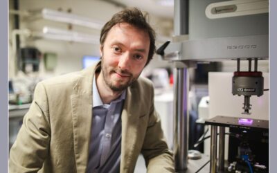
Yong Lei grew up in Hefei, the capital city of the Anhui province in China and pursued his early education in semiconductor physics at the Sun Yat-Sen University. Following his doctoral research at the Chinese Academy of Sciences, he moved to Germany in 2003, where he worked at the Karlsruhe Institute of Technology as an Alexander von Humboldt Research Fellow.
With an outstanding research record in the area of nanostructuring, a topic which was quite new and off the beaten track then, his career took off as a group leader at the University of Muenster, where he was soon promoted to the rank of junior professor in 2009. Since joining Technical University of Ilmenau as a professor and head of the Applied Nano-Physics Research Group in 2011, he has been working tirelessly on the development of advanced 3D nanostructured materials for energy conversion and storage.
We caught up with Lei to talk about his journey into STEM, his passion for research, and the world of patterned nanomaterials.
Who are the people that may have encouraged or inspired you to enter a challenging STEM field?
From middle school, my parents were always encouraging me to become a researcher of the natural sciences, although at that time, my favorite subjects were literature and history. My father was a famous architect in Anhui Province, and I guess maybe when he was young, he really wished to become a natural scientist, but he happened to become a successful architect and the only way to fulfill his childhood dream was to encourage one of his sons to follow that path.
Then, I selected physics as my major at Sun Yat-Sen University, which is one of the top national universities in China. After four years of studying physics, my interest in sciences became much higher than before, and finally I decided to pursue my Ph.D. at the Institute of Solid State Physics (ISSP) in CAS.
What inspired you to choose your current line of research?
When I just started my postgraduate research in 1996 at the ISSP, my supervisor, Professor Li-de Zhang, inspired me to choose nanostructuring using AAO templates as my doctoral research topic. It was a new topic at that time, focusing on complicated electrochemical processes, and no one had ever worked on it in the institute. I found the topic was challenging in terms of the limited experimental conditions of the institute, but it also made it very interesting and attractive to me.
What do you feel has been your greatest accomplishment?
From early on in my scientific career, when I was a postdoc in 2001, I realized that surface nano-patterning, as the key to achieving device miniaturization on the nanoscale, still lacked an efficient technique to prepare large-scale ordered arrays of surface nanostructures.
I had the idea that a very thin type of AAO template could be used for surface nano-patterning. After a few months of working, I found the idea was not just attractive but also crazy: many technical points needed to be solved, especially how to transfer an ultra-thin anode aluminum oxide (AAO) template (1 cm2 with only 200 nm thickness) onto a substrate without breaking.
I kept working on it until all the technical points were solved, which occurred in 2004 and gave it the name “UTAM surface nano-patterning”. Nowadays, the UTAM technique has been accepted as an efficient nano-patterning technique.
Despite this extended function of the AAO template, it could only be used to prepare 1D structures and planar 2D patterns, which is still far from satisfactory regarding the requirements of many devices, which require 3D structures to fully utilize all dimensions for device functionalization.
Right after the UTAM concept was well-established in 2007, I realized that 3D nanostructuring should be the next crucial functional evolution of the AAO template. After a few years of work in my group, a complete 3D-nanostructuring technique was accomplished, and was used for constructing energy conversion and storage devices like batteries, supercapacitors, and photoelectrochemical cells [for solar power].
What advice would you give to your younger self or new researchers entering the field?
My advice to young researchers is, the motivation of your research or selecting your topic should be not (just) for a good job or a better career, but rather as a hobby. You should really have curiosity and interest in what you are doing now. Don’t always follow the fashionable topics, and do what you really wish to research.
What future discovery or achievement would you most like to see?
Within the realm of 3D and multiple nanostructuring, the AAO template technique has been revolutionary and has broadened in the past years. However, I do believe that we are still not reaching (or maybe far away from) the zenith of its potential, such as completely controlling all the structural aspects of arrayed nanostructures. But with constant effort, [I believe] it is possible.
What are your future plans?
I will continue to work on template nanostructuring techniques and hopefully realize an “ultimate nano-structuring” concept for complete geometric and property control of arrayed nano-components with multi-functionalization and applications.
What are your interests outside of the lab?
Yes, a good work/life balance is important for a researcher. My hobbies outside of my research are diverse, such as reading historical books, enjoying pop music, playing billiard with friends, and taking vacations where I can drive my racing car at high speeds on the German highways.
To learn more about Lei’s work and his review on 3D Nanostructures, read the paper published in Advanced Energy Materials, which is part of a recent Virtual Issue “10 Years of Advanced Energy Materials Research” celebrating the 10th anniversary of the journal.