Weather results from a complex interplay of physical phenomena. On the nanoscale, functional materials can act in a similar way, which often impacts their performance.
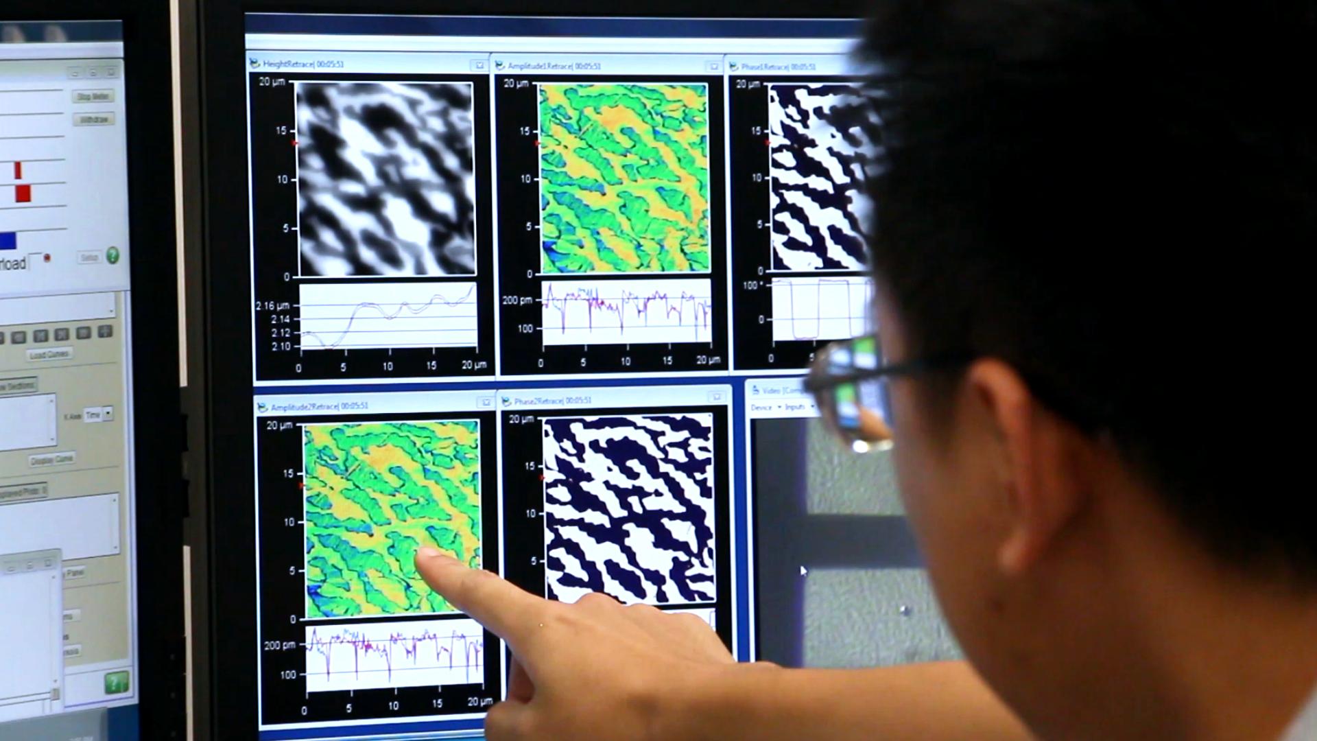
In Advanced Materials, Prof. Kaiyang Zeng and his colleague from the National University of Singapore discuss how local multifield coupling phenomena (MCP) in materials can be investigated by scanning probe microscopy (SPM) techniques.
Prof. Kaiyang Zeng: “Understanding MCP has great scientific and engineering significance, as materials and devices are often operated under a combination of multiple physical fields and working environments. The materials response to the synergetic effects of the multifield determine the functionalities, performance, and lifetime of the materials, and can even influence how it is manufactured.
On the nanoscale, a single external stimulus can cause complex phenomena to occur, which can change the performance of the material. For example, when an external electric field is applied to ZnO the dipoles reorient, which in turn affects resistive switching behavior.
To study MCP, SPM can be used. The atomically sharp tip used in SPM provides resolution down to the atomic scale, making localized characterization of different physical properties at the same location in the material possible.
In the future, MCP should be characterized by a combination of novel SPM experiments, theoretical methods, and machine-learning-assisted data analysis.”
To find out more about characterizing MCP in materials, please visit the Advanced Materials homepage.


