 With the ongoing miniaturization in electronics, the dimension of functional elements becomes so small that their properties are basically controlled by interfaces. One convenient way to control the characteristics of interfaces is to use molecular (mono)layers, which can even adopt the role of functional components in devices. In particular, organic self-assembled monolayers (SAMs) are highly promising candidates in the field of molecular electronics. The electronic properties of these molecular layers play a crucial role for device characteristics and therefore engineering of energetics and orbital localization are highly desirable.
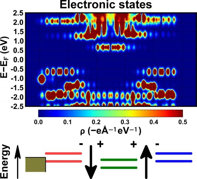
Egbert Zojer and his research team have developed a modular concept to design organic SAMs with user-defined properties. Their idea is based on providing a toolbox of functional elements comprising polar, semiconducting, radical, and H-bonding building blocks as well as anchoring groups to build SAMs of controlled orbital localization and energetics. As an exemplar case, conjugated thiols that can be bonded to gold surfaces are discussed. Key of the presented approach are collective electrostatic effects resulting from the parallel alignment of dipolar units within the backbones of the SAM-building molecules. These collective effects can be exploited to locally control the electrostatic structure of a SAM. Quantum-mechanical calculations reveal that by coupling dipolar with semiconducting building blocks, quantum-cascades and monolayer-based quantum-well structures can be realized, allowing for control of the local electronic structure and a localization of electronic states. In addition, strategies to induce spin sensitivity in particular regions of organic monolayers by adding neutral radical segments into SAMs are presented.
It is noteworthy that the proposed toolbox can be easily expanded, for instance by introducing alternative functional elements or by varying the bandgap of the semiconducting elements. While challenging to realize experimentally, the results presented demonstrate the great potential of such a toolbox to manipulate the electronic properties of interfacial layers.
Advanced Science is a new journal from the team behind Advanced Materials, Advanced Functional Materials, and Small. The journal is fully Open Access and is free to read now at www.advancedscience.com.