Between the generation and consumption of electrical energy, electrical power must change its form several times. After more than 40 years of development, present-day silicon devices have reached their physical limitations.
Alternatively, gallium nitride (GaN) possesses superior material properties which have the potential to reduce the size and weight of devices up to a factor of 10 as well as significantly increase energy efficiency.
To compensate for higher material costs, GaN can be grown in thin layers up to a few micrometers thick on top of Si substrates. However, this requires an insulating buffer that isolates the active GaN part from the Si substrate.
Empirically well-known, carbon dopants make GaN insulating but at the same time can “trap” electrons for certain durations and change electrical characteristics such as the resistance of the device. Thus, the goal of a collaboration of researchers from Austria was to clearly identify the role of carbon and the electrical behavior of carbon-doped layers.
To further complicate matters, high-quality carbon-doped GaN can only be grown on Si with a complex multilayer stack in between. This does not allow the distinction between the behavior of this multilayer and the actual carbon-doped layer.
In contrast to former investigations, the authors developed test structures that allowed for investigations of single GaN layers. Therefore, the key was the insertion of a highly n-doped layer between the multilayer and the carbon-doped layer which behaves as a back electrode as well as a layer that maps the reaction of the above carbon-doped layer to an applied external bias.
Starting from the sophisticated electrically and optically characterized test structures, the researchers derived a physical model for carbon-doped GaN that explains the actual role of carbon and is superior to previous models.
They discovered a key feature of the insulating behavior, namely that carbon occupies two different sites in the crystal, causing Fermi-level pinning. The model further shows that electron trapping in carbon defects is not only detrimental, as often thought, but also makes multilayers consisting of carbon-doped and undoped layers far more insulating than each layer on its own, as was then experimentally proven.
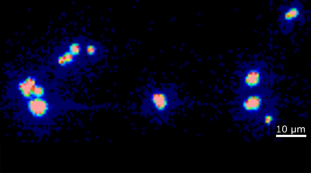
Investigated test structures also revealed a breakdown-like phenomenon that is distinguished by metastable current filaments and a negative differential resistance region.
The lead author, Christian Koller of KAI GmbH Villach, believes that their research “is the first step to deeply understand what a perfect GaN buffer should look like, why it behaves as it does, and how to conduct analyses on it—without being forced to rely on fully empirical development. Pioneering the frontier of new physics, this research furthers the push to unleash GaN’s full potential.”
The research was published as an Editor’s Choice article and will be included in a forthcoming special issue on Advances in Physics of Semiconductors in physica status solidi (b).


