Surely by now researchers should know everything there is to know about silicon. However, recent results have disrupted what we thought we knew about the element, and, in particular, its surfaces.
Silicon was first identified in 1824 by the Swedish chemist Jöns Jacob Berzelius. It is the seventh most abundant element in the universe and by mass, the second most abundant element in the Earth’s crust. Interest in silicon picked up in the mid 1950s when silicon transistors were developed to replaced vacuum tubes. It became the preferred material for electronic devices due to its very low power consumption and our ability to fabricate small circuits and integrate them functionally on small chips.
Silicon has ushered in what is known as “the silicon revolution”, which has transformed our society and pervades every corner of our daily lives. When one refers to “semiconductor technology”, it is all about fabricating electronic devices on a silicon crystal, which is usually sliced off a big crystal to form thin wafers. This has enabled enormous computing capabilities that have reshaped our world by allowing us to process vast amounts of data, and has provided continuous access to valuable information.
While crystalline silicon has been long studied, surfaces as well as thin layers of silicon also play an important role in technology advancements, as here lies the “active” element in all electrical devices. In the 1970s, there was tremendous interest and research going on to understand the atomic structure and electrical properties of silicon surfaces, as their fundamental properties were still unknown and widely debated.
Studying silicon surfaces
I came to work at IBM’s Thomas J. Watson laboratory in 1972 to help develop and apply new techniques to study surfaces but had done my Ph.D. work on metal surfaces. I continued to work on metal surfaces as they were well understood, thereby facilitating the development of these new techniques. Back then I was an outsider to silicon surface research. During a presentation to Frank T. Cary, the IBM CEO at the time, Mr. Cary asked me why I was not studying silicon surfaces. I thought, yes, why not? And when the opportunity arose to do a new type of measurement that no one had done before, I saw my chance.
In my new effort to study silicon surfaces, I was involved in understanding the structure and electronic properties of Si100 and Si111 surfaces — surfaces that had been widely studied since 1957 but whose structure was never understood. Here the 100 and 111 designations refer to the angle at which a crystal is cut and later polished to leave a flat plane of atoms on the surface. Of course, these surfaces have to be cleaned and heated to high temperatures to remove debris and allow the surface atoms to organize, like marbles all stacked together in different arrangements.
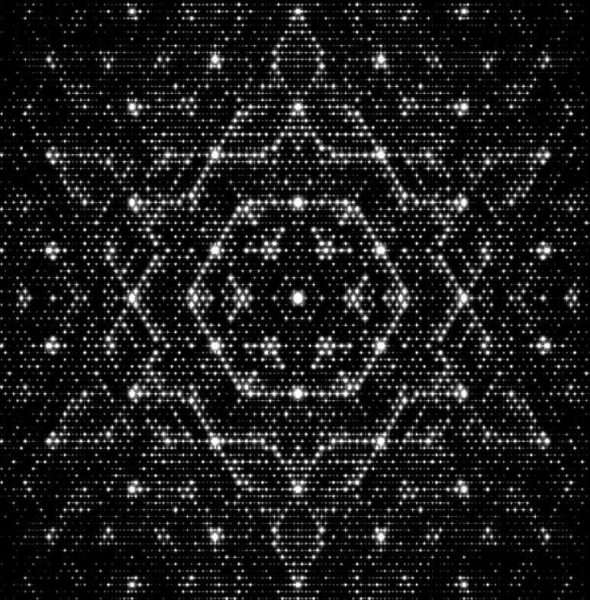
A recent discovery, discussed later in this article, was based on these first studies of the Si111 surface. The annealed Si111 surface exhibits a 7×7 diffraction pattern, which is derived from the unusual atomic structure it possesses. This pattern captivated all who viewed it and the 7×7 became undoubtedly the most widely studied semiconductor surface, bar none.
It was after 1980 when I developed the capability to study silicon surfaces over a wide temperature range (from 1200–15 K), which allowed me to study more properties of the 7×7 surface. What people had known around that time was that if one fractured a bar of crystalline silicon along the 111 direction, one obtained a simple 2×1 diffraction pattern, and upon heating the 2×1 surface in an ultra-high vacuum momentarily above about 800 K, the surface formed the 7×7 pattern and was very stable. A theoretical model of the 2×1 structure was proposed and established around 1983, but structure and chemical nature of the 7×7 surface was much more complex and elusive.
My new temperature-dependent measurements of the 7×7 showed many new interesting electronic transitions that were not previously observed, but more importantly, they revealed that the surface became insulating at lower temperatures below about 50 K. Ordinarily, if the surface was a semiconductor, it would be expected to become an insulator at low temperatures. But the surface was not semiconducting but metallic! Having electrons at the surface go from being metallic to insulating is a very unusual effect that depends on how the electrons spins align themselves. Generally such behavior has a specific temperature dependence, but a different temperature dependence was found for the 7×7.
Unresolved paradoxes in the 7×7 silicon surface
In 1985, a simple atomic model of the bonding and structure of the 7×7 was proposed, which fit diffraction experiments. Finally in 2000, when calculations had matured and could be performed to predict the complex structure of the 7×7 surface, they all indicated that the 1985 7×7 structure was confirmed to be the lowest energy (most stable) structure. The problem was that this calculated structure was always metallic, which was in contradiction to all experiments. This became an unresolved paradox of the silicon 7×7 surface.
Another paradox of the 7×7 was also found in 1986 through new measurements performed with IBM colleagues, Bob Hamers and Ruud Tromp, using a new device I had designed with the intention of doing electron spectroscopy on silicon surfaces, but with atomic resolution. This was an advanced design of what is called a scanning tunneling microscope or STM for which other IBM colleagues in Zurich shared the 1986 Nobel Prize in Physics.
The higher stability of my STM design allowed us to see the electron clouds at different locations about the various surface atoms and resolve their energies — all atomically resolved. These experimental measurements and their interpretations were initially valid in terms of simplified calculations, and again in 2000 with extensive first principle quantum mechanical calculations. However, the theory did not predict one of the surface states I had observed in 1983 and then again with atomic resolution in 1986. During this time, several researchers confirmed this new electronic state, but no one had a clear explanation of it either. This too, like the insulating ground state, became another paradox of the 7×7 surface.
Getting back in the game after 25 years
In 1993, I left the laboratory to pursue other interests. I retired completely in 2005 to a paradise-like environment in Florida. However, one can only catch so many fish or play so many rounds of golf before the boredom sets in — especially if your golf game seems to be getting worse, not better!
Fast forward to 2017 when my grandchildren asked, “What did you do when you were young?” But the clincher came when my daughter also asked, “Gee, dad, what did you do?”
That is when I decided to write down for my grandchildren why I became a scientist, what I did and what is was like being a scientist. Even after all that time, I remembered these old paradoxes, skeletons in the closet of surface science so to speak, and was curious as to what ever became of them.
To my surprise, they were never resolved despite many new studies. After spending two years studying all these past results and catching up with the literature, I discovered why these two paradoxes, as well as more recent ones, were arising. Again, these paradoxes were all based on the fact that many experiments were now telling us something different than what state-of-the-art theoretical calculations were telling us.
Answers to long-standing questions
This discovery occurred through a process of reverse engineering by trying to consider alternate structures that might account for certain features; there were many structures that were proposed over the years that would not fit either. To my surprise, I found a new structure which did account for all the unusual paradoxes. The trick was that for very complex systems there can be different arrangements of atoms that from one angle look the same as another structure but are bonded together differently, almost like ice cream cones stacked upright on a tray. Looking down on them for atop, they are spheres, up close some may have sprinkles, and looking from the side one sees they are actually on a cone.
The details of this new structure give it markedly different properties. Now its bonds were more two-dimensional and differed from those proposed in the original 1985 structure. As a result, the electrons behaved very differently since they were localized in this new 2D framework rather than being an extension of the bulk (3D) structure as proposed in 1985. After 2000, everyone in the scientific community still believed that the original 1985 structure was correct.
By about 2008, many of the researchers doing surface work had switched over to studying the properties of 2D materials, the most famous of which is graphene. Graphene differs chemically from graphite (it’s bulk form) even though these two materials are both carbon-based and whose atoms are both arranged in hexagonal structures. But because the carbon atoms in graphene have double bonds (sp2 bonds) and graphite does not, this dramatically changes how its electrons behave. As a result, graphene possesses a whole new range of unusual properties, the most notable being very high electron mobility, which is important for electrical devices.
In 2010 the discovery of graphene was awarded the Nobel Prize in Physics. And by that time, major efforts were underway to adapt these and other 2D structures for electrical devices. However, such efforts proved problematical since forming graphene on a substrate for very large-scale integrated applications was very difficult and costly to implement for commercial use.
In the search for promising new electronic materials, in 2012 it was discovered that one could form a 2D structure analogous to graphene using silicon. This was done by growing a monolayer of silicon on a silver surface. This monolayer of 2D silicon grown on silver showed several properties analogous to graphene and was called silicene. However, the role of the silver surface was questioned as well as whether the 2D character of the silicon atoms were preserved on silver, especially as the silicon layers became thicker.
The big surprise came when the new structure that I discovered showed many similarities to the 2D structure of silicon on silver. The new 7×7 structure contains the same honeycomb framework of silicon atoms as is found in silicenes and displayed some of the same unusual magnetic features observed in silicene nanoribbons. I was also able to apply some of the fundamental principles of quantum mechanics to explain why the atoms in the 7×7 organized the way they did on a honeycomb lattice and what was responsible for the unusual temperature dependent change I had originally observed 37 years ago! (Quantum mechanics was developed and formalized from 1905–1930 to understand the unusual behavior of the smallest particles of matter, atoms and electrons — a behavior that does not occur for large objects that we are all familiar with.) Perhaps because silicon atoms are the seventh most abundant atoms in the universe and naturally organized to form the 7×7 structure, it became 777, my lucky number! You just cannot argue with mother nature on such coincidences!
A more complete understanding of such new silicon surface structures and their properties are needed to verify and apply these findings. Nevertheless, this new conclusion resolves many past paradoxes of the nature of silicon surfaces and reveals the 7×7 to be a new 2D material. This study is a first step forward in a direction that may usher in a new era for 2D silicon technology. Since it is such a change in conventional thinking, one that has been prevalent in the community for the past 30 years, these results will no doubt be very controversial. Resolving such mysteries is part of the excitement that occasionally occurs in science. And yes, even now, silicon appears to be an element of surprise!
References:
Nobel Prize in Physics for Graphene (2010)
Nobel prize In Physics for Development of Electron Microscopy and the STM (1986)
J.E. Demuth, Evidence for Symmetry Breaking in the Ground State of the Si(111) – 7×7: The Origin of its Metal-insulator Transition, Physica Status Solidi (b) – Basic Solid State Physics (2020) DOI: 10.1002/pssb.202000229
J.E. Demuth, Experimental Evidence for a New 2-D Honeycomb Phase of Silicon: A Missing Link in the Chemistry and Physics of Silicon Surfaces?, Journal of Physical Chemistry C (2020). DOI: 10.1021/acs.jpcc.0c04860
P. Vogt, et al., Silicene: Compelling Experimental Evidence for Graphenelike Two-Dimensional Silicon, Phys. Rev. Lett. (2012). DOI: 10.1103/PhysRevLett.108.155501
J. E. Demuth,et al., Temperature-Dependent Surface States and Transitions of Si(111)-7×7, Phys. Rev. Lett. (1983). DOI: 10.1103/PhysRevLett.51.2214
B. N. J. Persson and J. E. Demuth, Inelastic scattering of slow electrons from Si(111) surfaces, Physical Rev. B (1984). DOI: 10.1103/PhysRevB.30.5968
R. J. Hamers, R. M. Tromp, and J. E. Demuth, Surface Electronic Structure of Si (111)-(7×7) Resolved in Real Space, Phys. Rev. (1986). DOI: 10.1103/PhysRevLett.56.1972
R.J. Hamers, J.E. Demuth, and R.M. Tromp, Electronic and Geometric Structure of Si(111)-7×7 and Si(001) Surfaces, Surface Science (1987). DOI: 10.1016/0039-6028(87)90176-2