Imagine that instead of having to pay a hefty bill after dropping your phone and cracking its screen, your phone simply repaired itself. The application of self-repairing electronics is expansive, from more durable robots to self-repairing satellites to self-healing screens.
What used to be the dreams of science fiction authors could soon become reality thanks to researchers from Technion – Israel Institute of Technology.
The team, led by Yehonadav Bekenstein from the Faculty of Material Sciences and Engineering and the Solid-State Institute at the Technion, have reported in Advanced Functional Materials an eco-friendly, self-healing nanocrystal semiconductor. “Our research focuses on structural reconstruction of defects, which is enhanced in halide perovskites due to the high mobility of atoms and restoration of broken bonds,” wrote the team in their paper.
Halide perovskite nanocrystals have already drawn significant attention within the field of materials science due to their unique properties, which makes them highly efficient in energy conversion while remaining inexpensive to produce. The current study focuses on a category of perovskites called double perovskites — toxic-free alternatives to commonly used lead halide perovskites.
“Metal halide perovskites are known to be very sensitive to water and decompose, releasing the toxic lead into soil or drinking water, for example, for a cracked solar cell exposed to rain,” said Bekenstein in an email. “The European Union restricts the use of such devices. Here we use lead-free materials, which are a greener and safer option for these applications.”
It appears that as a result of a happy coincidence, the team discovered this interesting phenomenon. When observing their perovskite nanoparticles under a transmission electron microscope (TEM), the electron beam caused defects in the nanocrystals.
“[While] we were investigating the structure of the double perovskite nanocrystals using a TEM microscope, we were surprised when we saw void-defects (holes) forming inside the particles and moving around,” explained Bekenstein. “Although this phenomenon is not new and occurs in many materials, voids usually do not move. We were intrigued by the exciting dynamics presented by these voids and decided to explore it further. It was a happy accident!”
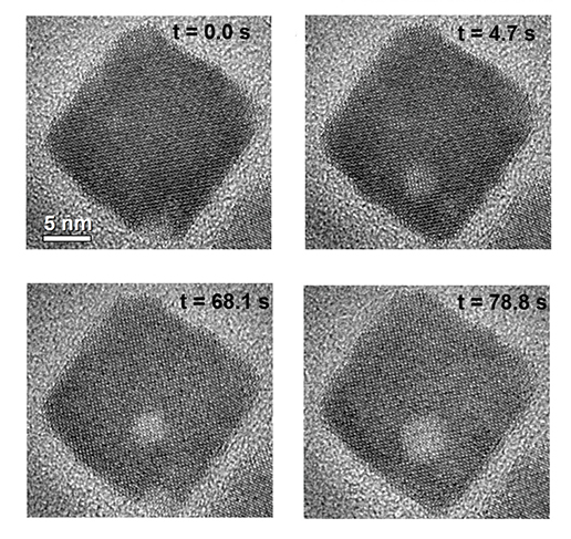
Under the microscope, the holes forming in the double perovskite, where alternating Ag+ and In3+ cations replace Pb2+, were observed to move within the crystal, forming first on the surface then moving inwards, toward more energetically stable locations.
The scientists noticed that the nanocrystals’ surface structure plays an important role in the dynamics of these holes once they form. The internalization, they hypothesize, occurs as a result of organic molecules that coat the nanocrystals’ surface.
“We figured out that we could engineer this effect and even reverse it by tweaking the surface energy of the crystal,” said Bekenstein. “In nanocrystals, it is known to be related to organic molecules that cover their surface. We removed some of those molecules and saw the self-healing properties of the double perovskite crystals.”
When they removed the organic molecules, instead of moving the holes inside, the crystals spontaneously ejected the them, returning to their original structure and in essence, repairing themselves — though this does lead to structural degradation over time.
This study, says Bekenstein, is an important step towards understanding the processes that enable perovskite nanoparticles to heal themselves and paves the way for their incorporation into more durable and sustainable solar panels, electronic devices, and more.
“There is a long way to go and many adjustments to acquire the ability to produce them on an industrial scale,” said Bekenstein. “To make a difference, one must demonstrate the same effect on bigger crystals and macroscopic layers. This is the crucial next step.”
Reference: Sasha Khalfin, et al., Self-Healing of Crystal Voids in Double Perovskite Nanocrystals Is Related to Surface Passivation, Advanced Functional Materials (2021). DOI: 10.1002/adfm.202110421