 Using bundles of vertical zinc oxide nanowires, researchers have fabricated arrays of piezotronic transistors capable of converting mechanical motion directly into electronic controlling signals. The arrays could help give robots a more adaptive sense of touch, provide better security in handwritten signatures and offer new ways for humans to interact with electronic devices.
The arrays include more than 8,000 functioning piezotronic transistors, each of which can independently produce an electronic controlling signal when placed under mechanical strain. These touch-sensitive transistors – dubbed “taxels” – could provide significant improvements in resolution, sensitivity and active/adaptive operations compared to existing techniques for tactile sensing. Their sensitivity is comparable to that of a human fingertip.
The vertically-aligned taxels operate with two-terminal transistors. Instead of a third gate terminal used by conventional transistors to control the flow of current passing through them, taxels control the current with a technique called “strain-gating.” Strain-gating based on the piezotronic effect uses the electrical charges generated at the Schottky contact interface by the piezoelectric effect when the nanowires are placed under strain by the application of mechanical force.
“Any mechanical motion, such as the movement of arms or the fingers of a robot, could be translated to control signals,” explained Zhong Lin Wang, a Regents’ professor and Hightower Chair in the School of Materials Science and Engineering at the Georgia Institute of Technology. “This could make artificial skin smarter and more like the human skin. It would allow the skin to feel activity on the surface.”
Mimicking the sense of touch electronically has been challenging, and is now done by measuring changes in resistance prompted by mechanical touch. The devices developed by the Georgia Tech researchers rely on a different physical phenomenon – tiny polarization charges formed when piezoelectric materials such as zinc oxide are moved or placed under strain. In the piezotronic transistors, the piezoelectric charges control the flow of current through the wires just as gate voltages do in conventional three-terminal transistors.
The technique only works in materials that have both piezoelectric and semiconducting properties. These properties are seen in nanowires and thin films created from the wurtzite and zinc blend families of materials, which includes zinc oxide, gallium nitride and cadmium sulfide.
In their laboratory, Wang and his co-authors – postdoctoral fellow Wenzhuo Wu and graduate research assistant Xiaonan Wen – fabricated arrays of 92 by 92 transistors. The researchers used a chemical growth technique at approximately 85 to 90 degrees Celsius, which allowed them to fabricate arrays of strain-gated vertical piezotronic transistors on substrates that are suitable for microelectronics applications. The transistors are made up of bundles of approximately 1,500 individual nanowires, each nanowire between 500 and 600 nanometers in diameter.
In the array devices, the active strain-gated vertical piezotronic transistors are sandwiched between top and bottom electrodes made of indium tin oxide aligned in orthogonal cross-bar configurations. A thin layer of gold is deposited between the top and bottom surfaces of the zinc oxide nanowires and the top and bottom electrodes, forming Schottky contacts. A thin layer of the polymer Parylene is then coated onto the device as a moisture and corrosion barrier.
The array density is 234 pixels per inch, the resolution is better than 100 microns, and the sensors are capable of detecting pressure changes as low as 10 kilopascals – resolution comparable to that of the human skin, Wang said. The Georgia Tech researchers fabricated several hundred of the arrays during a research project that lasted nearly three years.
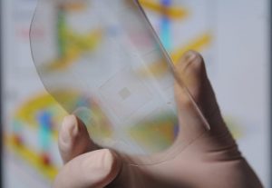
The arrays are transparent, which could allow them to be used on touch-pads or other devices for fingerprinting. They are also flexible and foldable, expanding the range of potential uses.
Among the potential applications:
Multidimensional signature recording, in which not only the graphics of the signature would be included, but also the pressure exerted at each location during the creation of the signature, and the speed at which the signature is created.
Shape-adaptive sensing in which a change in the shape of the device is measured. This would be useful in applications such as artificial/prosthetic skin, smart biomedical treatments and intelligent robotics in which the arrays would sense what was in contact with them.
Active tactile sensing in which the physiological operations of mechanoreceptors of biological entities such as hair follicles or the hairs in the cochlea are emulated.
Because the arrays would be used in real-world applications, the researchers evaluated their durability. The devices still operated after 24 hours immersed in both saline and distilled water.
Future work will include producing the taxel arrays from single nanowires instead of bundles, and integrating the arrays onto CMOS silicon devices. Using single wires could improve the sensitivity of the arrays by at least three orders of magnitude, Wang said.
“This is a fundamentally new technology that allows us to control electronic devices directly using mechanical agitation,” Wang added. “This could be used in a broad range of areas, including robotics, MEMS, human-computer interfaces and other areas that involve mechanical deformation.”
Source: Georgia Tech