The growing functional range of smartphones, digital cameras and tablets requires a high level of integration density in the semi-conductor field and the miniaturization of electronic modules. Until now, the use of faster microchips was virtually impossible due to increased heat generation. This problem can now be resolved.
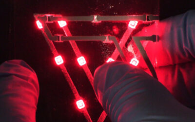
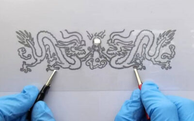
The company Akon developed a novel etching technology that permits the production of traces with a width of just 20µm in homogeneous quality over an entire panel. For comparison purposes: a human hair is approx. five times as thick. The special feature: the micro-fine surface structures are so smooth that this also results in the additional optimization of the signal quality.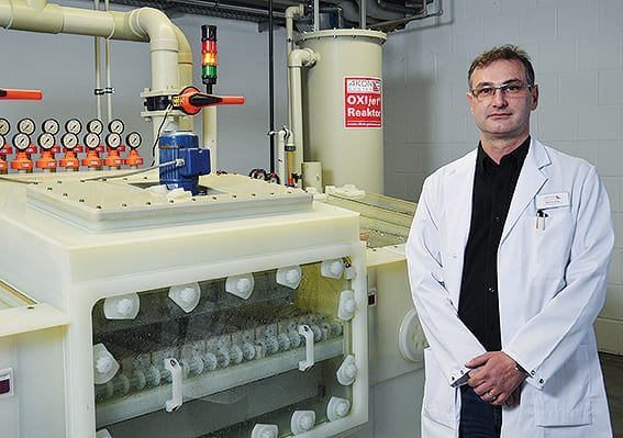
“The patented Axon Oxijet process is a milestone in the development of mobile communications. The scope of functions of mobile end-user units largely depends on micro-conductor technology and the miniaturization of contact surfaces.” explains Marcus Lang, Technical Manager at Akon.
According to Akon, the process used so far has the disadvantage of having a very broad process window which results in an unstable and hard-to-control etching process. This has a negative effect on the etching quality of the structures to be formed. This causes a high production scrap rate. The Oxijet process enables a really small process window and accurate metering of the etching solution. The positive effects on the surface structure of the traces can be seen in the steepness of the etched flanks, finer structures and increased signal quality. The production yield increases as a result, which brings about a reduction in costs in this hard-fought market.
In the manufacture of printed circuit boards, the conducting structures are etched onto a copper surface in a complex and expensive process. Up to now, liters of hydrogen peroxide (H2O2) were used in these etching processes. The problem is that H2O2 is a very strong oxidation agent which increases the risk of fire and can cause severe damage to the eyes and irritation to the skin. It is also toxic.
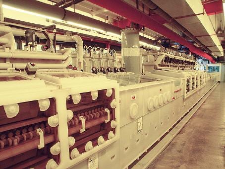 It is precisely here that the novel technology is setting new standards, because this flammable toxic material is replaced by ozone (O3) that is generated “in situ”. The process generates ozone from ambient air using a generator. The ozone is introduced into the production cycle directly at the point it is required. The volume of ozone generated in this way is of the order of a few grams. Excess ozone is converted to oxygen in a catalytic converter and then discharged back into the air. The critical and expensive handling of the toxic material hydrogen peroxide is completely eliminated.
“Using this process not only protects the environment but also offers the electronics industry a quantum leap in the reduction in the surface area of printed circuit boards in series production. New developments that so far have been unthinkable will now become possible. Increasing the pack density makes electronic modules faster and more powerful. Developers and programmers are able to set out upon entirely new paths to create new generations of equipment.” adds Managing Director Wolfgang Dambacher.
Images: AKON GmbH