Layered crystals can be envisioned as a nearly endless reservoir of atomically thin layers that are weakly stacked together by so called van-der-Waals interactions. These interactions are basically the social distancing equivalent of chemical bonds, where no directionality is present and weak physical interactions hold atoms together without forming a true bond.
Since van-der-Waals interactions are weak, atomic layers within a crystal can be pulled apart with ease, ultimately allowing one to peel down the structure to a single layer. These single layers are not only the thinnest 2D entity of the layered crystal, but also show exiting physical properties due to this reduced dimensionality.
The 2D character of these materials makes them sensitive to their environment as there is no “bulk” to take a punch. From a practical standpoint, this allows scientists to control charge flow in downscaled device architectures — a feat which might help overcome the current limits of miniaturization faced by conventional silicon semiconductor technologies, where proper control of charge flow (on vs. off) is becoming more and more difficult in ever shrinking transistors.
This all began with the discovery of graphene, which single-handedly started one of the most popular research fields in modern solid-state physics, culminating in the Nobel prize in Physics in 2010. Remarkably, graphene was peeled into existence with simple scotch tape in a process known as exfoliation, and showed physical properties unique to its thinned-down structure. This completely changed the perception of layered crystals, shifting focus onto the exfoliated layers and opened numerous possibilities for an armada of excited physicists and materials scientists who, armed with scotch tape, set out to exfoliate everything under the sun.
In recent years, the “scotch-tape method” enabled a ton of research on 2D materials and has led to some of the most exciting discoveries made in materials science. While this method truly qualifies as a game changer on the research level, exfoliated flakes are usually very small and their yields are equally limited. Nevertheless, the promise for technological exploitation has elevated the need for a scalable supply of single layer materials.
While over the years different approaches have been developed to effectively grow or isolate crystal layers, exfoliation still provides the highest quality products; but more scalable approaches are needed beyond just scotch tape.
It therefore became apparent to think about stickier surfaces for exfoliation by considering the chemistry of the targeted layers. On this note, gold was investigated as a very sticky surface for a prominent family of layered materials called transition-metal dichalcogenides (TMDCs). These chalcogen-terminated layers earned their popularity due to their promise as 2D semiconductors, which can switch conductivity on and off, something that has been difficult to realize in graphene.
The “stickiness” of gold came as no surprise to researchers since it is known to exhibit strong interactions with chalcogen atoms, especially sulfur. It turned out that gold could peel the outermost layer of the bulk crystal with high success rates, leading to large-scale single layers whose size depended on the interface area between gold and the parent crystal. This bypassed the limitations of the less glamorous (and herein less sticky) scotch tape while retaining the high quality originating from the single-crystalline starting material.
In a recent article published in the journal pss RRL, a gold-mediated exfoliation enabled by low-temperature “baking” was reported, which overcomes the limitations of previous “press-and-peel” methods. This simple modification potentially increases the range of conditions and materials for which gold-mediated exfoliations can be used, enabling 2D materials to finally leave the lab.
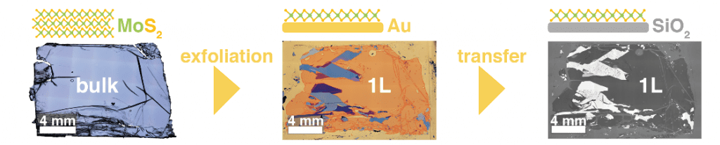
The template-strip method uses a silicon wafer coated with gold, which can be stripped off the wafer template to produce batches of (literally) wafer-scale gold. Hypothetically, this method was expected to proceed by simply pressing the gold onto a suitable layered crystal. However, in the real world, hardly anything goes as planned and no exfoliation occurred at room temperature.
This is surprising but, fortunately, was easily solved by baking the gold-layered-crystal-sandwich. The heat initiates the exfoliation and allows the gold to exfoliate ultra-large sheets of MoS2, the most prominent member of the TMDC family, which was used in a proof-of-concept experiment. This simple modification boosted the overall robustness of the exfoliation process and since temperatures and the baking time are low, it could be very valuable for future industrial applications.
The strong gold-TMDC interactions — gold’s stickiness — are a double-edged sword since the exfoliated layers are difficult to remove after baking and get stuck on the gold surface. In previous studies, an etching step is used to wash away the gold and free the exfoliated monolayer for use in technologically relevant substrates. An accompanying transfer process, which usually uses polymeric membranes to host layers during the transfer, relocates any exfoliated flakes from the gold to the desired target substrate without losing, damaging, and/or wrinkling the layer. While useful, the atomically thin, smooth surfaces of the single layers are sensitive to contaminations by the polymeric residues from the transfer membrane. We therefore thought: What if gold’s role in the process can be extended beyond just exfoliation to aid in the transfer of the layers?
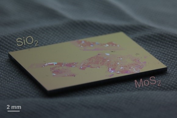
A unique transfer approach was therefore developed where the gold used in exfoliation is freed from its substrate stack and the resulting gold foil hosts the exfoliated materials during their transfer onto the target substrate, almost like decorating it with leaf gold. The foil is then etched away, leaving behind the atom-thick layers at their target destination, such as on a silicon wafer.
Besides a glamorous re-interpretation of scotch tape for exfoliation, this study could help to render gold-mediated exfoliations more robust and applicable in an industrial context. Furthermore, since gold also proved its capability for clean transfer processes, it is even more qualified to lead 2D materials one step closer to industrialization – i.e., using gold to “pull off” the next big innovation in tomorrow’s electronics.
Written by Max Heyl and Emil List-Kratochvil
Reference: Max Heyl, et al., Thermally Activated Gold‐Mediated Transition Metal Dichalcogenide Exfoliation and a Unique Gold‐Mediated Transfer, pss (Rapid Research Letters) (2020). DOI: 10.1002/pssr.202000408