Researchers with the US Department of Energy’s Lawrence Berkeley National Laboratory have discovered why graphene’s electron conduction can’t be completely stopped, an essential requirement for on/off devices.
The on/off problem stems from monolayers of graphene having no bandgaps – ranges of energy in which no electron states can exist. Without a bandgap, there is no way to control or modulate electron current and therefore no way to fully realize the enormous promise of graphene in electronic and photonic devices. The Berkeley Lab researchers have been able to engineer precisely controlled bandgaps in bilayer graphene through the application of an external electric field. However, when devices were made with these engineered bandgaps, the devices behaved strangely, as if conduction in those bandgaps had not been stopped. Why such devices did not pan out has been a scientific mystery until now.

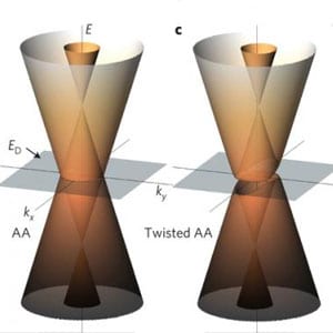
The Dirac spectrum of bilayer graphene when the two layers are exactly aligned (left) shifts with a slight interlayer twist that breaks interlayer-coupling and potential symmetry, leading to a new spectrum with surprisingly strong signatures in ARPES data. Image: Keun Su Kim, Fritz Haber Institute
Working at Berkeley Lab’s Advanced Light Source (ALS), a DOE national user facility, a research team led by ALS scientist Aaron Bostwick has discovered that in the stacking of graphene monolayers subtle misalignments arise, creating an almost imperceptible twist in the final bilayer graphene. Tiny as it is – as small as 0.1 degree – this twist can lead to surprisingly strong changes in the bilayer graphene’s electronic properties.
“The introduction of the twist generates a completely new electronic structure in the bilayer graphene that produces massive and massless Dirac fermions,” says Bostwick. “The massless Dirac fermion branch produced by this new structure prevents bilayer graphene from becoming fully insulating even under a very strong electric field. This explains why bilayer graphene has not lived up to theoretical predictions in actual devices that were based on perfect or untwisted bilayer graphene.”
Monolayers of graphene have no bandgaps – ranges of energy in which no electron states can exist. Without a bandgap, there is no way to control or modulate electron current and therefore no way to fully realize the enormous promise of graphene in electronic and photonic devices. Berkeley Lab researchers have been able to engineer precisely controlled bandgaps in bilayer graphene through the application of an external electric field. However, when devices were made with these engineered bandgaps, the devices behaved strangely, as if conduction in those bandgaps had not been stopped.
To get to the bottom of this mystery, Rotenberg, Bostwick, Keun Su Kim of the Fritz Haber Institute in Berlin and their colleagues performed a series of angle-resolved photoemission spectroscopy (ARPES) experiments at ALS beamline 7.0.1. ARPES is a technique for studying the electronic states of a solid material in which a beam of X-ray photons striking the material’s surface causes the photoemission of electrons. The kinetic energy of these photoelectrons and the angles at which they are ejected are then measured to obtain an electronic spectrum.
“The combination of ARPES and Beamline 7.0.1 enabled us to easily identify the electronic spectrum from the twist in the bilayer graphene,” says Rotenberg. “The spectrum we observed was very different from what has been assumed and contains extra branches consisting of massless Dirac fermions. These new massless Dirac fermions move in a completely unexpected way governed by the symmetry twisted layers.”
Massless Dirac fermions, electrons that essentially behave as if they were photons, are not subject to the same bandgap constraints as conventional electrons. In their research, the scientists state that the twists that generate this massless Dirac fermion spectrum may be nearly inevitable in the making of bilayer graphene and can be introduced as a result of only ten atomic misfits in a square micron of bilayer graphene.
“Now that we understand the problem, we can search for solutions,” says Kim. “For example, we can try to develop fabrication techniques that minimize the twist effects, or reduce the size of the bilayer graphene we make so that we have a better chance of producing locally pure material.”
Beyond solving a bilayer graphene mystery, Kim and his colleagues say the discovery of the twist establishes a new framework on which various fundamental properties of bilayer graphene can be more accurately predicted. “A lesson learned here is that even such a tiny structural distortion of atomic-scale materials should not be dismissed in describing the electronic properties of these materials fully and accurately,” he says.


