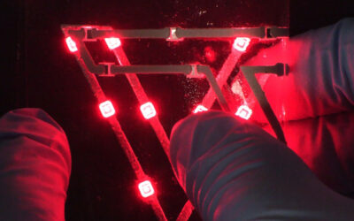
Images of an organic-based electrical device on a highly flexible, stretchable, and patchable freestanding polymeric substrate.
The development of flexible electronic devices continues to advance at great speeds. In fact, a flexible electronic device may soon be coming to a pocket or bag near you in the form of a bendable smartphone or tablet. Despite this rapid progress, there is still a notable gap in the field. For stretchable and patchable systems, most reported devices use inorganic rather than organic components. A major hurdle for organic-based devices is their difficult preparation; typical patterning and photolithography preparative methods are expensive and time-consuming. Despite this challenge, organic materials still offer major advantages over their inorganic counterparts (e.g., cost, availability, and tunability). This gives the search for economical and efficient preparative methods a special significance.
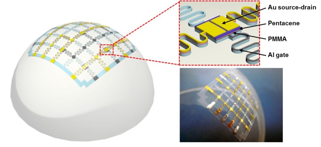
Now, a major breakthrough is reported in the Journal of Polymer Science B: Polymer Physics, by Prof. Soonmin Seo and co-workers at Gachon University and Pukyong National University in Korea. In the report, they describe a new method for preparing electrical circuits composed of organic devices on structured freestanding polymeric substrates that are highly flexible, stretchable, and patchable. Using this novel technique, they prepare and study integrated organic thin-film transistors (OTFTs) and organic photovoltaic (OPV) devices. The polymeric substrate is composed of a UV-curable (~ 365 nm) polyurethaneacrylate (PUA) mixture on a polydimethylsiloxane backbone. The structure of the patterned substrate contains three areas; small plates, spring-shaped bridges, and connecting pieces. As Seo and co-workers write, “The small plates ((1 mm × 1 mm) on which the organic devices are fabricated are connected with the neighboring plates, using the spring-shaped bridges (of 150 mm width), and the connecting pieces (of 275 mm radius). The connecting pieces are used to compose the substrate with a larger number of spring-shaped bridges, to improve the mechanical strength of the substrate; and the spring-shaped bridges play a key role in enhancing the flexibility and stretchability of the PUA substrate. Since the spring-shaped bridges significantly relieve the force being applied to the small plates, the small plates are substantially free from the structural stress and strain that accompany substrate deformation. The dimension, shape, and composition of the substrate can be tuned for specific purposes in the photoresist patterning process. The polymeric bridges and the connecting pieces also facilitate the fabrication of flexible and stretchable electrodes, without additional photolithography or patterning processes.”
Schematic illustration of organic thin-film transistors fabricated on the polyurethaneacrylate substrate.
Having ready access to the PUA substrate, the Korean team turned its attention to device fabrication. Their first target was an integrated OTFT, which was constructed using electrodes (Al and Au), and poly(methyl methacrylate) and pentacene as the dielectric and active layers, respectively. Measurements of the device’s field effect transistor properties showed little decrease upon stretching. “The averaged hole mobility of the devices slightly changed by less than 4.5% upon the 70% lateral stretches, whereas no significant change (less than 1% in the averaged hole mobility) was observed during the lateral stretches up to 30% These results imply that the force being applied to the PUA plate according to lateral stretches is completely relieved by the spring-shaped bridges in the small strain region. Further tests of the OTFT system on a hemispheric plate again confirmed that deformation (bending in this case) of the substrate has little effect. “The average hole mobility of the devices changed by less than 9% after 100 consecutive cycles of freestanding bending”.
The PUA substrate’s high transparency (a transmissivity of ~90% in the range of 300–1100 nm) makes it ideal for photovoltaics, which was the second class of device prepared in the study. Bulk-heterojunction OPV devices were constructed with a poly(3,4-ethylenedioxythiophene)-poly(styrenesulfonate) buffer layer, a photoactive layer comprising C61-butyric acid methyl ester, poly(3-hexylthiophene-2,5-diyl), and an Al electrode. The PUA substrate, covered with indium tin oxide, completed the system. The PUA-based OPV device was then tested on a glass slide and a plastic hemisphere. Compared to the glass slide, the properties [(Voc), short circuit current (Jsc), fill factor (FF), and power conversion efficiency (PCE)] on the plastic hemisphere were slightly lower by a few percentage points. This finding was expected considering the glass slide’s higher transmittance compared to the plastic hemisphere. Although more work will be needed to optimize the devices, a path for new, highly flexible optoelectronic devices is now clearly open.
Seo and co-workers conclude by saying, “We anticipate that these results will be applied to the development of various flexible, stretchable, and patchable organic devices and integrated circuits, which can lead to further applications in many fields of science and engineering.”