Every year, almost two million tons of electronic scrap are produced in Germany. Printed electronics enhance the trend to throw used devices away by reducing production costs and opening up new markets with disposable items, such as interactive packagings or smart band aids. Young researchers at Karlsruhe Institute for Technology (KIT) have therefore developed printed electronics made of compostable natural materials and processes for industrial production
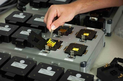
Organic light-emitting diodes (OLED) can be produced easily and at low cost. Thanks to compostable materials, they are also made sustainable. (Photo: KIT).
The young researchers make devices using easily biodegradable materials, such as semiconductors and dyes made of plant extracts or insulators made of gelatin. “These may not be as long-lived as the inorganic alternatives, but they easily survive the service life of disposable electronics,” says Dr. Gerardo Hernandez-Sosa, leader of the Biolicht Young Investigator Group of KIT. After use, he says, the electronics can simply be thrown away into the biowaste bin or on compost heaps, where it will rot like a banana skin.
Starch, cellulose, or chitin are suited as carrier foils, for instance. The scientists use very little metals or metalloids, such as silicon. The advantages of plastic materials: They are bendable, cheap, and can be processed into miles of printing foil. By means of this technology, it is possible to produce on the industrial scale e.g. stickers with an electronic traffic light indicating shelf life or band aids with incorporated sensors to monitor the healing process.
First, electronic components have to be printed onto the compostable foils similar to letters onto paper. Their function depends on the ink used: Instead of dye particles, conducting, semiconducting or non-conducting, i.e. insulating, materials are dissolved in the ink. For the inks however, the young scientists now have to identify environmentally compatible materials with the desired electrical properties.
The Biolicht Young Investigator Group is affiliated to the KIT Light Technology Institute. Its laboratories are located at the InnovationLab, Heidelberg, an application-oriented research and transfer platform of science and industry. It is funded by Karlsruhe Institute of Technology, the companies of BASF SE, Merck, Heidelberger Druckmaschinen AG, and SAP AG, as well as by the University of Heidelberg.